 English
Power systems built around insulated-gate bipolar transistors (IGBTs) must balance switching efficiency, thermal performance, and electromagnetic compatibility (EMC). Fast switching helps reduce power losses, but it can also generate electromagnetic interference (EMI) that affects nearby circuits, sensors, and communication interfaces. Gate drivers play a central role in managing this trade-off. By controlling IGBT switching behavior and improving signal integrity, we can design power conversion systems that operate more reliably while meeting demanding EMC requirements.
At Firstack, we specialize in the research, development, and sales of power semiconductor drivers, power stacks, and testing equipment. Our digitally based gate driver solutions are designed to support reliable switching and help engineers address electromagnetic challenges in modern power electronics.
How Switching Creates Electromagnetic Interference
An IGBT switches high currents and voltages during turn-on and turn-off. Rapid changes in voltage (dv/dt) and current (di/dt) can excite parasitic inductance and capacitance in the power circuit, producing conducted and radiated noise. That interference may disturb control electronics or cause unwanted behavior in nearby components. EMC performance therefore depends not only on the IGBT itself, but also on the gate-drive circuit, layout, cabling, grounding, and filtering.
How Drivers Control Switching Transitions
A gate driver supplies and removes charge at the IGBT gate, determining how quickly the device changes state. A transition that is too fast can increase voltage overshoot, ringing, and high-frequency noise; one that is too slow can raise switching losses and device temperature. We need to balance these competing effects for the actual power module and operating conditions.
Engineers can tune the external gate resistance and, where the driver design allows, use different turn-on and turn-off settings. The goal is not simply to make switching slower, but to control the edge rate without creating excessive losses or stress. Mitsubishi Electric’s IGBT application guidance also emphasizes gate voltage, gate resistance, and circuit layout as key elements of drive design.
Reducing False Switching and Improving Signal Integrity
High dv/dt can couple through an IGBT’s Miller capacitance and raise the gate voltage of a device that should remain off. In a half-bridge, unintended turn-on can create shoot-through current, increasing electrical stress and potentially disrupting system operation. Suitable off-state gate bias, a low-impedance gate-emitter path, careful layout, and appropriate driver protection help limit this risk.
Digital control can also improve consistency in the way gate commands are processed. Our digitally based driver series is designed to offer lower electromagnetic interference than analog drivers, alongside reliability and configuration flexibility. This does not replace good PCB layout or system-level EMC testing, but it gives designers another useful element in a coordinated noise-control strategy.
Protection Features Support Stable Operation
Undervoltage can leave a power switch inadequately driven, while a short circuit requires a controlled response to limit stress. Protection functions such as undervoltage lockout (UVLO) and soft shutdown help manage these abnormal conditions. When evaluating IGBT gate drivers, engineers should confirm how faults are detected, how quickly the output responds, and whether shutdown behavior suits the module’s short-circuit limits.
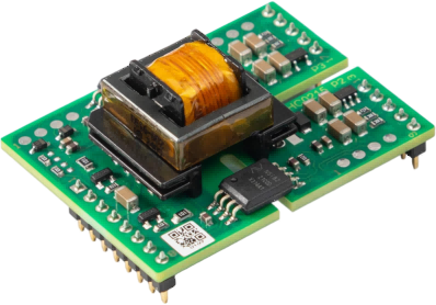
For example, one of our IGBT gate drivers, 2FHC0215C, supports IGBT modules up to 900 A/1700 V, uses a 15 V turn-on gate voltage, and provides dual channels with an electrical interface. It supports multilevel topology and includes short-circuit protection with soft shutdown, undervoltage protection, and active clamping. The product specification lists 2 W output power per channel and a peak gate current of 15 A.
Design the Whole System for EMC
Even a well-selected driver cannot compensate for poor power-stage design. Keep gate-drive loops short and compact, separate gate wiring from high-current paths, and minimize stray inductance. Place decoupling components close to the relevant supply pins, establish a deliberate grounding strategy, and evaluate shielding and filtering where measurements show they are needed. Check the complete assembly under realistic load and switching conditions rather than relying on component specifications alone.
Testing should cover both emissions and immunity. A design that passes one test setup may behave differently after cable lengths, enclosure panels, or grounding connections change, so repeat validation after significant hardware revisions. Use oscilloscope measurements to inspect gate voltage, collector-emitter voltage, and switching ringing, then conduct applicable EMC tests on the assembled equipment. If noise remains high, review switching resistance, cable routing, common-mode current paths, and enclosure bonding systematically instead of changing several variables at once.
Building More EMC-Ready Power Systems
Effective EMC design comes from coordinated choices: controlled switching edges, stable gate signals, appropriate protection, sound layout, and verification at system level. IGBT gate drivers are a key part of that process, but the best results come when engineers treat the driver and power stage as one design challenge.
At Firstack, we develop power semiconductor driver solutions for demanding power-electronics applications. Our 2FHC0215C combines a compact, dual-channel design with multilevel-topology support and protective functions for compatible IGBT modules. By selecting the right driver and validating the complete system, engineers can work toward reliable switching and stronger EMC performance without losing sight of efficiency, thermal limits, or application requirements.

