 English
A power semiconductor system can experience excessive switching losses, unstable waveforms, or unexpected temperature rises when its gate-drive circuit is not properly designed or configured. Overheating and ringing are two common symptoms that can indicate problems with switching speed, parasitic inductance, gate resistance, or circuit layout. Identifying the underlying cause is essential for improving efficiency, protecting power devices, and maintaining reliable operation.
At Firstack, we specialize in the research, development, and sales of power semiconductor drivers, power stacks, and testing equipment. Our digital gate-drive solutions are designed to support reliable switching and flexible integration. Understanding how to troubleshoot a MOSFET gate driver helps engineers distinguish between driver-related faults and problems originating elsewhere in the power circuit.
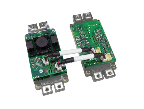
1. Identify the Root Cause of Overheating and Ringing
Before changing components, we recommend examining the gate-to-source voltage, drain-to-source voltage, and switching current with an oscilloscope. Observe both turn-on and turn-off transitions under controlled operating conditions. Confirm that measurements remain within the semiconductor manufacturer's recommended limits and use appropriate differential probes for high-voltage circuits.
Ringing often results from parasitic inductance interacting with the MOSFET's gate capacitances. Rapid changes in current or voltage can excite this resonant circuit, producing oscillations, voltage overshoot, electromagnetic interference, or unintended turn-on.
Overheating has several possible causes, including excessive switching losses, prolonged transition times, insufficient gate voltage, inadequate cooling, or unintended simultaneous conduction in a bridge circuit. The MOSFET gate driver itself may also dissipate excessive power if its output current, switching frequency, or load requirements are unsuitable.
2. Optimize Gate Resistance and Switching Speed
Gate resistance is one of the first parameters engineers should evaluate when troubleshooting ringing. A resistor that is too small may allow rapid gate-current changes and insufficient damping. Increasing resistance can reduce oscillations, but it also slows switching and may increase switching losses and device temperature.
We recommend testing resistance values incrementally while monitoring gate waveforms, drain-voltage overshoot, switching losses, and device temperature. Where the circuit permits, separate turn-on and turn-off resistors can help engineers optimize each transition independently. The final values should balance switching speed, efficiency, electromagnetic compatibility, and safe operating limits rather than simply eliminate visible ringing.
3. Improve PCB Layout and Power-Supply Stability
Poor layout can undermine even well-selected gate drivers. Long gate traces, large current-loop areas, and shared source inductance introduce parasitic effects that distort the effective gate voltage. We recommend keeping the gate-drive and return paths short, minimizing loop area, and placing gate resistors close to the power device.
A Kelvin source connection, when supported by the device package, can separate the gate-drive return from the main power-current path. This reduces the influence of source inductance on the control signal. Local decoupling capacitors should also be placed according to the gate drivers's datasheet recommendations to provide stable supply current during switching.
Next, verify the driver's supply voltage, grounding, input logic, and undervoltage lockout behavior. Supply dips or noisy control signals can interrupt switching or cause unexpected operation. When troubleshooting gate drivers, check whether ringing coincides with supply disturbances or switching-node transitions before attributing the problem solely to the output stage.
4. Check Miller Clamping and Protection Features
During fast switching, the Miller capacitance between the gate and drain can couple voltage transients into the gate. If the resulting voltage exceeds the device's threshold, the MOSFET may turn on unintentionally, potentially increasing losses or causing shoot-through in bridge configurations.
A Miller clamp provides a low-impedance path to hold the gate at its intended off-state potential. Engineers should confirm that the clamp is enabled where required and that its connection to the power device has sufficiently low parasitic impedance. Also verify undervoltage lockout (UVLO), fault responses, and isolation requirements against the manufacturer's documentation.
5. Select a Driver That Matches the Application
If layout improvements and parameter adjustments do not resolve the issue, reassess the driver's compatibility with the power semiconductor. Consider gate-charge requirements, peak output current, switching frequency, isolation rating, operating temperature, and protection functions. A driver that cannot supply the required gate current may produce slow transitions and excessive losses, while unnecessarily aggressive drive can worsen ringing.
At Firstack, we develop digital power semiconductor drivers designed for reliability, flexibility, and reduced electromagnetic interference compared with analog driver designs. Our 2FHC0240 gate driver core offers dual-channel operation, 2 W output power per channel at maximum ambient temperature, and a peak gate current of 40 A. It supports SiC modules rated up to 2300 V and incorporates reinforced insulation, Miller clamping, and UVLO.
These features make the 2FHC0240 a potential option for engineers evaluating high-voltage SiC applications. However, its suitability depends on the specific module, gate-charge characteristics, switching conditions, and system-level design. We recommend checking the product documentation and validating waveforms under representative operating conditions before deployment.
Build a More Reliable Switching System
Resolving overheating and ringing requires a systematic approach rather than a single component change. By measuring switching waveforms, tuning gate resistance, improving layout, checking supply stability, and validating protection functions, engineers can identify the underlying fault and reduce unnecessary power losses.
At Firstack, we focus on power semiconductor driving technology and supporting equipment to help engineers develop dependable power conversion systems. Choosing appropriate MOSFET gate drivers and carefully validating each design decision can improve switching performance, protect valuable semiconductor devices, and support long-term system reliability.

