 English
Insulated-gate bipolar transistors (IGBTs) have played a major role in the development of modern power electronics. By combining the gate-controlled operation of a MOSFET with the conductivity characteristics of a bipolar transistor, IGBTs offer a practical balance of controllability, current-handling capability, and conduction efficiency. Over several decades, improvements in chip structure, cell geometry, and manufacturing processes have expanded their applications in renewable energy, rail transportation, industrial motor drives, and power transmission.
Understanding the evolution of IGBT technology helps engineers evaluate device characteristics, identify suitable components, and anticipate future design requirements. At Firstack, we work across power semiconductor drivers, power stacks, and testing equipment, supporting engineers as power conversion systems become more demanding.
1. Early Planar IGBTs: Establishing the Foundation
Early commercial IGBTs used planar gate structures and punch-through (PT) designs. These devices offered voltage-controlled switching with lower drive-power requirements than traditional bipolar transistors, making them attractive for inverter and motor-control applications. However, early generations faced limitations in switching speed, conduction losses, and thermal stability when multiple devices operated in parallel.
Subsequent non-punch-through (NPT) designs improved ruggedness and provided more predictable temperature behavior. This development helped broaden the range of applications where IGBTs could be used, particularly in industrial equipment that required dependable switching under varying loads. The continuing challenge was to reduce conduction and switching losses without sacrificing blocking voltage or safe operating capability.
2. Field-Stop Technology and Thinner Wafers
A major step forward came with field-stop structures and thinner semiconductor wafers. By controlling the electric field near the collector side, field-stop designs allowed a thinner drift region while maintaining the required voltage-blocking capability. This reduced stored charge and helped shorten the current tail during turn-off.
Lower conduction voltage and reduced switching energy improved overall efficiency. These developments also enabled higher power density, allowing designers to achieve greater output capability without proportionally increasing semiconductor size.
3. Trench Devices and Modern IGBT Technology
Trench-gate structures changed the way the MOS channel is formed inside the chip. Instead of relying entirely on a planar gate arrangement, the gate extends into trenches in the silicon, enabling greater channel density and improved cell utilization. This can reduce conduction losses and support higher current density.
Combining trench gates with field-stop technology brought further improvements. Later generations refined cell geometry, wafer thickness, carrier distribution, and lifetime control to optimize the trade-off between conduction losses, switching losses, and ruggedness.
Modern IGBT technology is therefore not defined by trench geometry alone. Chip structure, diode characteristics, packaging, thermal performance, and application-specific optimization all influence the final device behavior. Engineers should compare complete datasheet parameters rather than assume that a newer generation automatically performs better in every operating condition.
4. Why Gate Driver Design Still Matters
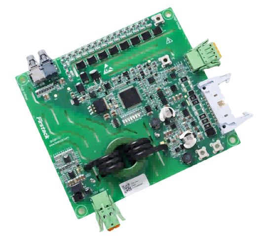
Even an advanced IGBT chip depends on its gate-drive circuit for controlled switching. An appropriately selected IGBT gate driver must provide the required gate voltage and current while managing switching speed, electrical isolation, and fault response. Incorrect drive conditions can increase switching losses, create excessive voltage overshoot, or compromise short-circuit protection.
Engineers should evaluate gate resistance, turn-on and turn-off behavior, undervoltage lockout, and protection timing alongside the semiconductor's operating limits. For high-power modules, layout parasitics and differences between parallel devices also deserve attention. A well-matched IGBT gate driver helps the power device operate closer to its intended performance while supporting reliable system operation.
At Firstack, we develop power semiconductor drivers, power stacks, and testing equipment for applications such as renewable energy, rail transportation, power transmission, and motor drives. Firstack have secured more than 150 intellectual property rights. Our work supports engineers evaluating switching performance and system-level integration.
Looking Ahead: Integrating Devices and Drive Systems
The evolution from planar structures to trench and field-stop devices demonstrates how improvements in semiconductor design can increase efficiency and power density. Yet successful implementation still requires coordination between the chip, driver, thermal system, and protection architecture.
At Firstack, we believe that understanding device characteristics and validating gate-drive performance are essential steps in modern power electronics development. By pairing an appropriate IGBT gate driver with the selected module and operating conditions, engineers can make better-informed design decisions and build power conversion systems that meet demanding efficiency, reliability, and application requirements.

