 English
Inverters rely on insulated-gate bipolar transistors (IGBTs) to convert electrical power efficiently in applications such as renewable energy systems, motor drives, rail transportation, and power transmission. However, electrical overstress, excessive temperature, incorrect switching, and inadequate protection can cause device failures that interrupt operation and increase maintenance costs. Understanding these failure mechanisms helps engineers develop more reliable power conversion systems. A properly selected IGBT gate driver supports this goal by controlling switching behavior, maintaining stable gate signals, and responding to abnormal operating conditions.
As a power semiconductor technology company, Firstack focuses on the research, development, and sales of power semiconductor drivers, power stacks, and testing equipment,and also can support the development of solutions for demanding power electronics applications.
1. Overcurrent and Short-Circuit Damage
Overcurrent is one of the most serious failure risks in inverter operation. It can result from load faults, wiring problems, switching errors, or a short circuit in the power stage. When current exceeds the device's safe operating limits, the semiconductor may experience rapid heating and destructive electrical stress.
A suitable IGBT gate driver helps manage this risk through short-circuit detection and rapid fault response. Depending on the design, desaturation detection or other current-monitoring methods can identify abnormal conduction. Soft shutdown can then reduce the gate voltage in a controlled manner, limiting excessive voltage spikes during turn-off. Protection settings must still match the module's short-circuit withstand time and the system's operating conditions.
2. Thermal Stress and Excessive Switching Losses
Excessive junction temperature can accelerate component degradation and eventually cause permanent failure. Common contributors include inadequate cooling, high ambient temperatures, excessive conduction losses, and switching losses caused by unsuitable drive settings. Repeated thermal cycling can also fatigue internal connections and solder joints.
We can help reduce avoidable switching losses by selecting appropriate gate-drive current and resistance. Stronger gate current can shorten switching transitions, but it may also increase voltage overshoot and electromagnetic interference. Engineers should therefore balance switching speed against thermal limits, voltage stress, and noise. Effective cooling and accurate thermal design remain essential because gate-drive optimization alone cannot eliminate overheating.
3. False Turn-On and Shoot-Through
When one switch turns on, rapid voltage changes can couple through the Miller capacitance of the opposite device, potentially raising its gate voltage. If both switches in a bridge leg conduct simultaneously, shoot-through current may flow directly through the DC link, creating severe electrical stress.
A well-designed driver helps prevent this problem through suitable off-state gate control, adequate gate-emitter voltage margins, and carefully managed switching timing. Dead time between complementary switching commands also reduces the risk of simultaneous conduction. Engineers should verify gate waveforms under realistic operating conditions, since parasitic inductance, layout, and operating voltage can influence unwanted turn-on.
4. Gate Overvoltage and Uncontrolled Switching
The gate-emitter voltage must remain within the device manufacturer's specified limits. Excessive voltage, ringing, or poor gate-loop design can damage the gate structure or produce unstable switching behavior. Similarly, insufficient gate voltage may prevent the device from conducting efficiently, increasing losses and temperature.
An appropriate IGBT gate driver supplies the required gate voltage while providing sufficient current for controlled transitions. Engineers should check positive and negative gate-voltage limits, power-supply stability, and the effects of parasitic inductance. Protective features such as undervoltage lockout (UVLO) can prevent operation when the drive supply falls below a defined threshold, reducing the risk of inadequately driven devices.
5. Why Driver Selection and System Design Matter
Preventing failures requires more than choosing a driver with a high output-current rating. Channel configuration, isolation requirements, protection functions, topology compatibility, and response characteristics must all suit the application. PCB layout, gate resistance, cooling, and fault coordination also influence the final result.
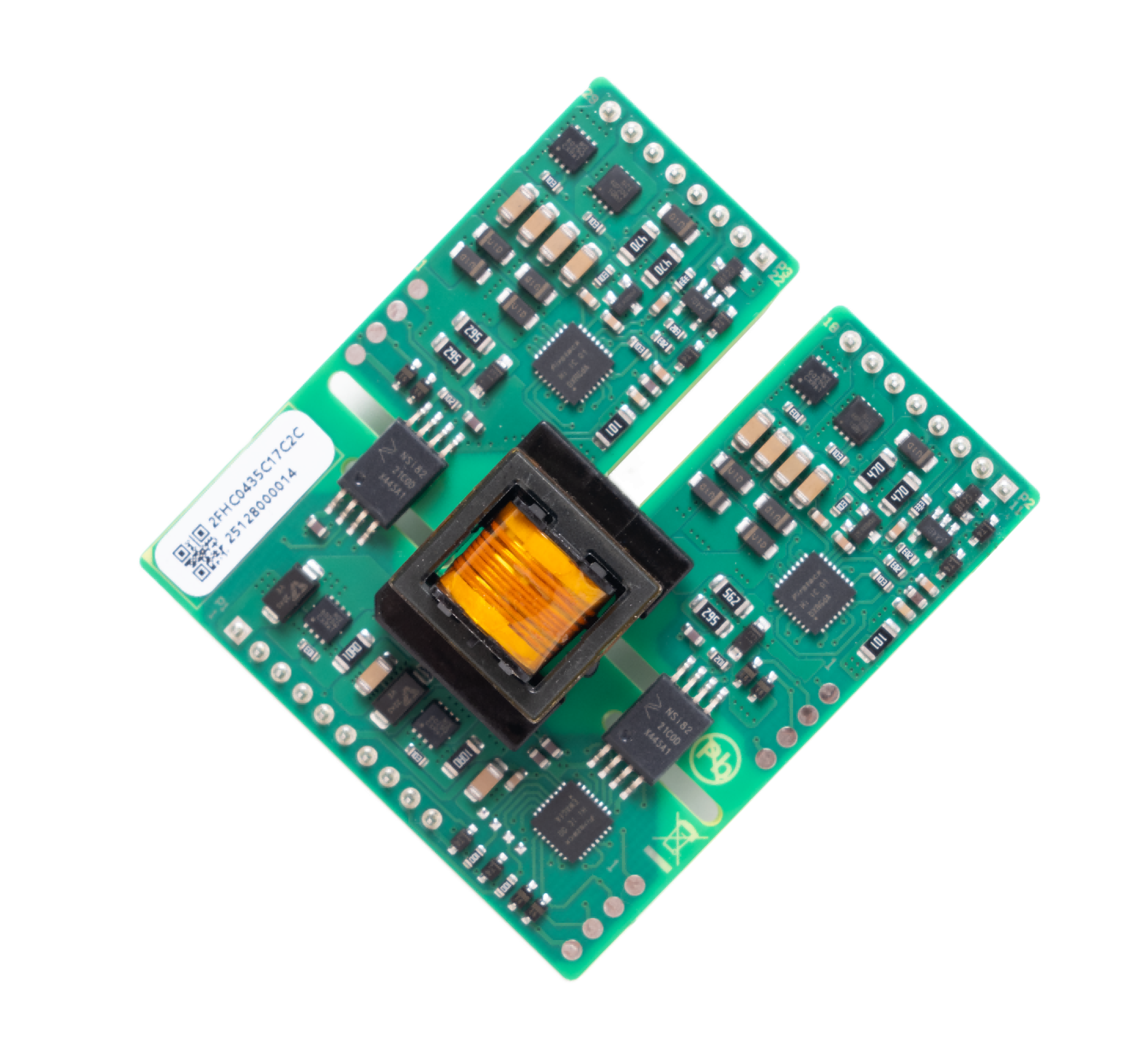
At Firstack, our 2FHC0215C gate driver core supports compatible power modules rated up to 900 A/1700 V. Its dual-channel electrical interface, 15 V turn-on gate voltage, multilevel-topology support, and intelligent fault management help engineers address practical power-stage requirements. The design also supports short-circuit protection, undervoltage lockout, and soft shutdown, providing useful functions for applications where switching reliability is critical.
Improving Inverter Reliability Through Better Drive Design
Inverter failures often result from interacting electrical, thermal, and control problems rather than a single component weakness. Overcurrent, overheating, false turn-on, and gate-voltage violations can all threaten long-term performance. Careful driver selection, coordinated protection, appropriate layout, and thorough testing help reduce these risks.
At Firstack, we develop power semiconductor driver solutions for applications including renewable energy, rail transportation, power transmission, and motor drives. By matching drive characteristics and protection functions to the selected module and system requirements, engineers can improve operational reliability while balancing efficiency, thermal performance, and electrical safety.

