In the previous two courses, we briefly introduced Miller clamping and short-circuit protection. This time, we first explore a core issue in SiC applications: circulating currents during SiC parallel operation.
1. The Influence of Circulating Current
Why focus on circulating current? When using IGBTs, we also encounter circulating current issues, but due to their slower turn-on speed (i.e., low dv/dt), this problem is not particularly pronounced. However, for SiC devices, the high-speed switching characteristics make circulating current issues especially significant.
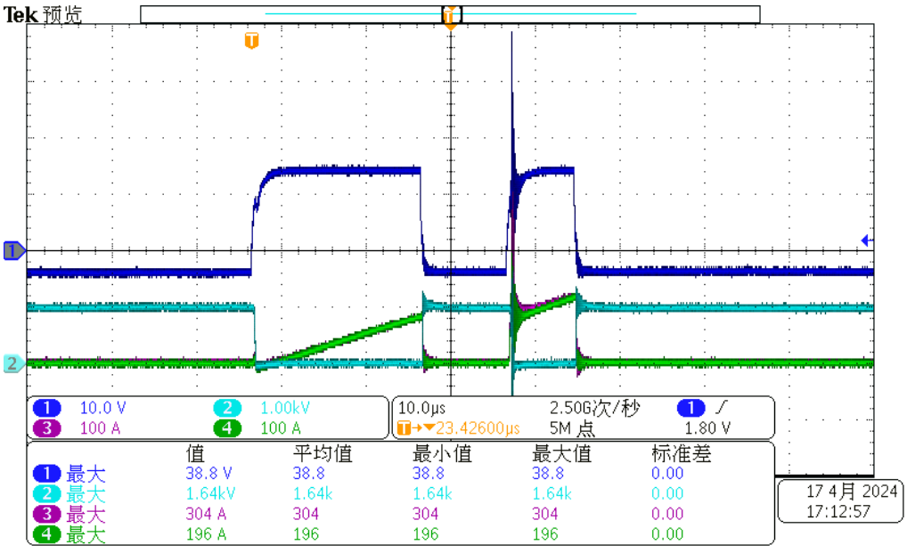
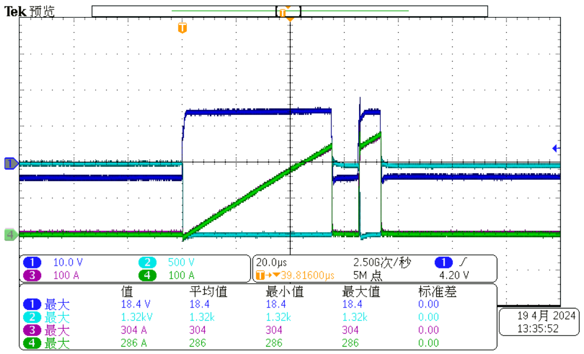
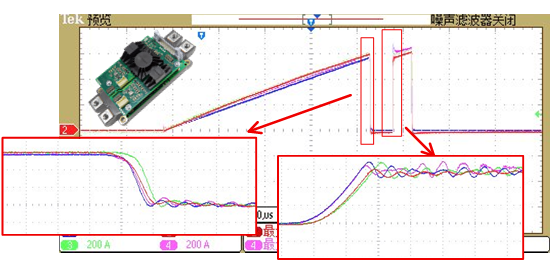
The figure below shows the test waveform of a SiC driver 2-in-parallel designed based on traditional IGBT drive scheme. When testing Module A, significant overshoot and oscillation in the gate voltage were observed at the instant of second turn-on, posing a risk of gate damage. Additionally, since even slight variations in the gate voltage VGS during turn-on can significantly affect the current, which also impacts current sharing efficiency, thereby reducing system stability and performance.
Therefore, it is necessary for us to investigate why this phenomenon occurs.
2.Where does the circulating current originate?
Circulating current is a complex issue involving both the drive circuit and the entire power circuit. Simply put, differences between modules and modules, circuits and circuits, lead to unexpected current.
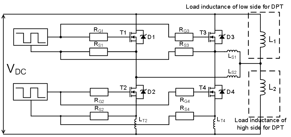
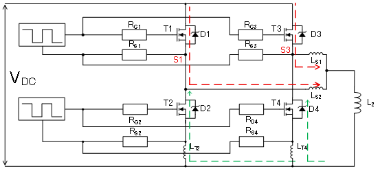
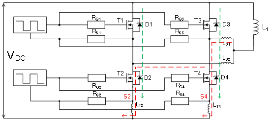
The figure below shows a typical 2-in-parallel drive circuit. T1 and T2 form one half-bridge, while T3 and T4 form another half-bridge. T1 and T3 are connected in parallel, T2 and T4 are connected in parallel. D1 to D4 represent the corresponding freewheeling diodes. RG denotes the gate resistor, and RS represents the discharge resistor between the gate and source terminals. LS denotes the stray inductance between the left and right half-bridges. LT represents the stray inductance at the sources of T2 and T4. L1 and L2 are the load inductance. When coming to circulating current, their essence lies in the gate voltage difference caused by the potential difference across the source due to stray inductance. IGBT modules exhibit low di/dt, whereas the di/dt of SiC can easily exceed 5000 A/μs, or even 10 kA/μs. Consequently, the impact of stray inductance is dramatically amplified.
We shall first analyze the switching process of the top bridge arm, which is most affected:
During the second turn-on process, T1 and T3 are on while T2 and T4 are off, then D2 and D4 enter the reverse recovery phase. The green arrows denote the reverse current paths. Variations such as inconsistent di/dt slopes, differing levels of stray inductance, and asynchronous turn-on will induce voltages with varying value and polarity across LS1 and LS2. Consequently, a voltage differential arises between S1 and S3. In practical testing, there are two primary scenarios.
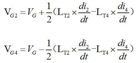
1. T1 and T3 cannot be turned on simultaneously. For example, turn-on thresholds differ due to chip inconsistencies. If T3 turns on before T1, the voltage of S3 would exceed that of S1, thereby forming a circulating current through RS3 and RS1. At this point, VS3 - VS1 = VLS1 + VLS2.
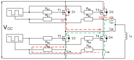
2.T1 and T3 may be turned on simultaneously. However, there is a performance disparity between the modules. At this juncture, the potential difference across S1 and S3 is:
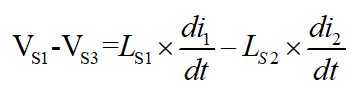
The voltage sharing across the gate driver depends on two critical factors: di/dt (the change rate of current) and LS (stray inductance). As di/dt can reach 10kA/μs level, this potential difference can be extremely large.
Due to the difference between LT2 and LT4, the red current depicted in the diagram flows through RS4 and RS2. At this point, the gate voltage of the bottom bridge arm may also experience positive or negative overshoot. The final voltage depends on the inherent characteristics of T2 and T4, as well as the stray inductance between LT2 and LT4. Consequently, for SiC parallel operation, Miller clamping serves as a crucial function to ensure stable gate voltage for the complementary switch.
The above analysis explains why gate voltage undergoes abrupt changes. Furthermore, there is numerous difficult-to-calculate parasitic capacitance both within the module and throughout the entire circuit, e.g., between the gate and heatsink, between the gate and source/drain and so on, which forms RCL resonant circuits. This results in the waveform we observe.
Throughout the entire process, how significant is the impact of the module itself on the results? Comparing the waveform above, we tested another B module under identical test conditions with the same gate driver, yielding the waveform below. We observe that the oscillations have markedly disappeared during the second turn-on, though a small peak remains. This confirms that the module itself exerts a substantial influence on the outcomes.
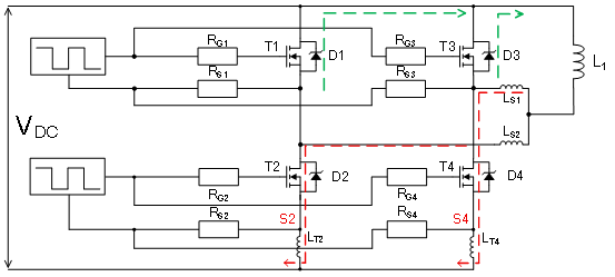
Here is the turn off process. The red arrow indicates the current during turn-on, while the green arrow represents the freewheeling path after T1 and T3 are turned off. Similar to the turn-on process, we must still consider two scenarios: one where the turn-off sequence differs, and another where simultaneous turn-off causes potential differences due to stray inductance and current slope. The second scenario is more akin to turn-on, where our primary focus remains on the turn-off sequence.
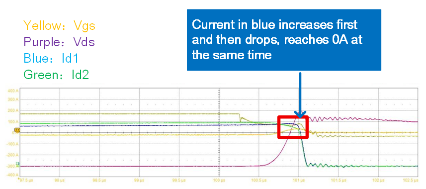
Assuming T1 turns off first and T3 later, the current reduced on T1 will increase on T3. At this point, due to the negative di/dt on LS2, a voltage with negative left and positive right polarity will be induced. On LS1, owing to the instantaneous increase in current, the voltage will be positive left and negative right. We observe that the gate voltage across T1, now superimposed with an additional positive voltage, slows its turn-off speed. Conversely, T3, with a superimposed negative voltage, turns off more rapidly. This creates a mechanism akin to negative feedback. Ultimately, the parallel modules achieve near-simultaneous turn-off. As illustrated in the waveform below, one module's current exhibits a noticeable rise at the turn-off instant, yet all modules ultimately switch off almost simultaneously.
Next is the analysis of the bottom bridge arm's turn-on and turn-off behaviour. Compared to the top bridge arm, the most significant difference in the bottom bridge arm lies in the change of reference ground: the source of the top bridge arm is connected to the drain of the bottom bridge arm, whereas the source of the bottom bridge arm is directly connected to DC-. Let us begin with the turn-on process. In the diagram below, the green arrows represent the freewheeling path of the top bridge arm, while the red arrows denote the currents through T2 and T4. It can be observed that regardless of the switching state of T2 and T4, the potential at their drains is affected, but the gate voltages of T2 and T4 themselves remain unaffected. The potential difference across S2 and S4 depends on the stray inductance LT2 and LT4 in the power circuit.
During the disconnection process, regardless of how T2 and T4 are turned off, the impact is primarily concentrated on LS1 and LS2. The polarity of the voltage across both LT2 and LT4 remains consistently aligned. Compared to the opposing voltage polarities in the top bridge arm, the overall risk in the bottom bridge arm can be considered lower than that in the top bridge arm.
The foregoing constitutes a concise analysis of circulating current during the turn-on and turn-off processes of parallel modules. Due to the presence of substantial parasitic capacitance throughout the circuit, such as CGS and CGD inherent to the gate itself, and even parasitic capacitance within the probes employed for measurement—the actual circuitry proves considerably more intricate. Nevertheless, the fundamental cause remains circulating current.
3.How to Suppress the Circulating Current
There are two key aspects to suppressing circulating current: drivers and modules.
Regarding drivers, the most crucial points are twofold:
Ensure signal consistency for parallel operation
Design specialized circuits to block circulating currents on the gate
For both customers and driver manufacturers, the first point is relatively straightforward to achieve. Whether using commercially available driver ICs or board-level drivers, good signal consistency can currently be attained. The primary challenge is the interrupt of the circulating current in the gate loop. At present, two main approaches are employed in design:
Each module employs an independent driver, with each driver receiving signals from the host computer separately.
A master-slave board architecture is adopted, whereby host computer signals are transmitted solely to the master board. Parallel operation is achieved by adding slave boards, with all slave board signals originating from the master board.
Firstack currently opts for the second approach based on its technological characteristics and drive reliability. The first approach demands exceptionally high signal consistency. The greater the number of parallel connections, the more challenging it becomes to ensure signal consistency across every driver. SiC devices typically turn on around 100ns, meaning a mere 10ns variation can severely impact parallel performance. Furthermore, during full-system operation, high temperature significantly affects device consistency, necessitating component screening when employing this method. However, its advantage lies in the fact that each driver operates independently, thereby eliminating any circulating current issues.
The second approach ensures excellent signal consistency. However, the challenge lies in isolating the circulating current at the source. As the source is connected to the driver power supply, power isolation must be implemented on each slave board. Firstack SiC gate drivers are based on proprietary parallel solutions, which have been thoroughly validated in customer installations.
The diagram below depicts 2FHD0620 4-in-parallel dual pulse test, employing EconoDUAL™ modules, though these were not subjected to any screening process. The four sets of signals represent the Id. Throughout the test, our driver not only achieves simultaneous switching of parallel modules but also demonstrates excellent suppression of circulating currents, as evidenced by the absence of significant current oscillations during the entire process.
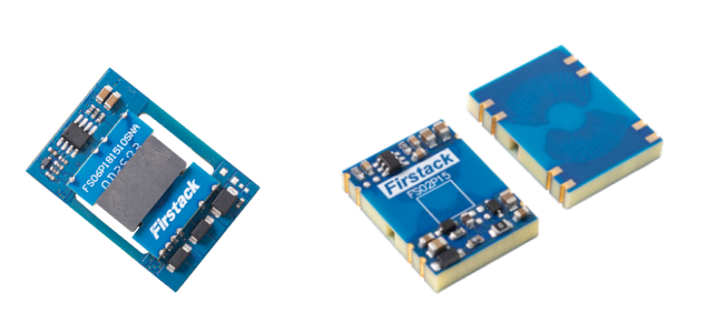
In addition to EconoDUAL™, Firstack also offers parallel solutions for Linpak and XHP2. What if discrete components such as TO247 or modules from the Easy series are used? Firstack can also provide the FS02P and FS06P power modules for SiC driver designs. Their exceptionally low primary-secondary coupling capacitance ensures power supply stability and extremely low common-mode noise.
For modules, consistency screening is of paramount importance. There are two key parameters:
1. Vgs(th), the gate threshold voltage directly impacts the consistency of parallel module switching
2. Rds(on), influences current distribution during both dynamic and static conditions
The effect of Vgs(th) is quite straightforward, but just how significant is the impact of Rds(on)?
Suppose there are two parallel modules with corresponding on-resistance values R1 and R2, both experiencing a voltage drop of V. The current distribution ratio is then:
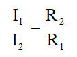
Under normal circumstances, the ratio is 1:1. If both R1 and R2 exhibit deviations of ±Δ = 10%, the formula becomes:
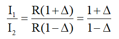
At this point, the current ratio becomes 1.22, representing a 22% current imbalance. Even with a ±Δ=5% tolerance, the current deviation reaches 10%. What if we have N modules connected in parallel? The formula can then be simplified to:
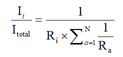
Itotal is the total current. Based on the on-resistance of each module, we can calculate the specific current allocated to it.
In summary, parallel-connected SiC modules must undergo consistency screening to ensure performance. Firstack has introduced the corresponding product ME100D/S-AM for SiC module screening. It can accurately detect the static characteristics of modules, helping users efficiently and conveniently complete module matching.
4.Other Issues When Connecting in Parallel
Besides the issues mentioned above, what else should we be mindful of when using SiC in parallel?
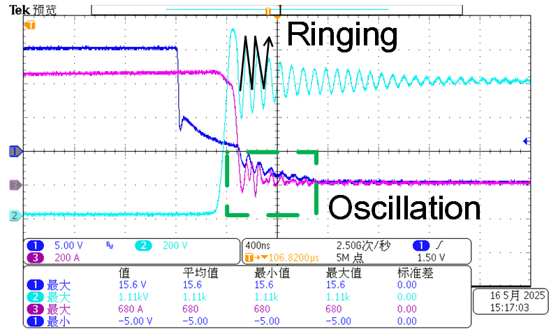
1. We must distinguish between ringing and oscillation. A key characteristic of ringing is its relatively fixed frequency and amplitude that decays regularly over time. Comparing the gate voltage or other electrical parameters of parallel modules reveals in-phase oscillations. Oscillation, however, often involves variable frequency and amplitude, with non-in-phase oscillations observed across the parameters of parallel modules. Therefore, observing ringing is not cause for concern, as it merely indicates significant parasitic parameters in the circuit. Oscillation, however, may stem from issues in the driver design or the module's inherent performance and warrants heightened vigilance.
2. When using SiC modules in parallel, the symmetry of the power circuit significantly impacts overall system performance. For example, in an AC output array, if the stray inductance on the AC-side current paths of the two modules differs, current sharing will be poor.
3. The probe used during testing is critical. Standard differential probes must never be used. Due to their wide measurement range, their accuracy is easily compromised when measuring oscillations in gate voltage. We recommend ground loop isolation probes and optically isolated probes. Simultaneously, the bandwidth of both the probe and oscilloscope is crucial. We recommend using a bandwidth of 800MHz or higher to obtain a relatively accurate waveform.
Conclusion
Parallel-connected SiC drives impose higher demands on both module and busbar design. Firstack is committed to providing customers with comprehensive power solutions—from drivers to modules to assemblies—delivering complete and reliable products and services. Interested parties are welcome to inquire at any time.