The commonly available board-level driver cores typically integrate four components:
- Power supply
- Isolation (power + signal)
- Driver
- Protection
What remains to be addressed before full deployment? How to design the peripheral circuitry?
Principle
The peripheral circuit comprises primary and secondary sections.
I. Primary Side
1) Fault Output
The core board's inherent fault signal is an open-drain (OD) output requiring pull-up via resistor and diode. Pull-up logic: High indicates normal operation; low indicates fault.
2) PWM Signal
An RC filter circuit is incorporated to ensure signal input quality and enhance operational stability.
II. Secondary Side
1) Short-Circuit Detection Circuit
For desaturation detection in low-voltage (≤1700V) modules common in industrial control applications, Firstack recommends a diode detection circuit.
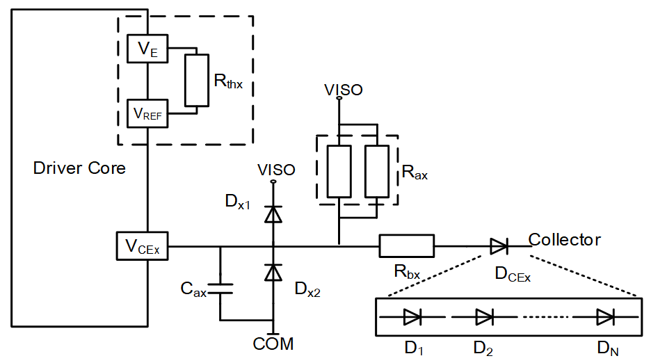
Principle of Diode Desaturation Detection
When the IGBT is off, the internal MOSFET in the driver connects VCE to VCOM. At this point, the VCax voltage equals the negative supply voltage.
When the IGBT is on, VISO charges Cax via Rax. If the IGBT saturates, the collector potential drops to VCEsat, and the VCax remains at a low level due to DCEx clamping.
Should the IGBT desaturate due to a short circuit, the VCE rises rapidly, the high-voltage diode DCEx turns off, VISO charges Cax. When the Cax potential reaches the detection threshold (set via the REF pin; refer to the product application manual for configuration), the internal ASIC comparator activates, triggering the soft-off MOS to turn off the IGBT.
2) Active Clamping Circuit
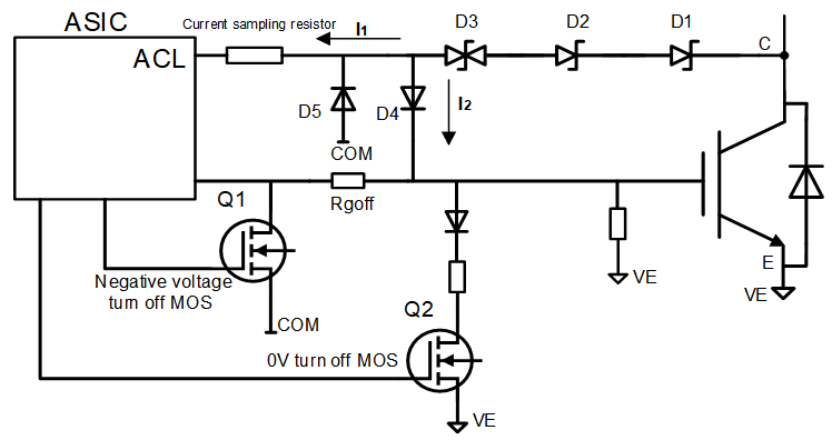
TVS (D1, D2, D3) and diodes (D4, D5) are connected in series to form an active clamping network. The diagram above is for reference only. The quantity and specifications of series components should be selected according to actual operating conditions. Under identical overall threshold conditions, increasing the number of TVS can enhance active clamping efficiency.
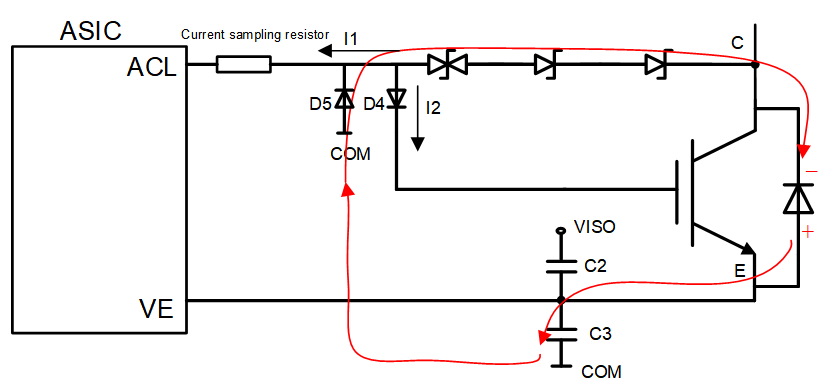
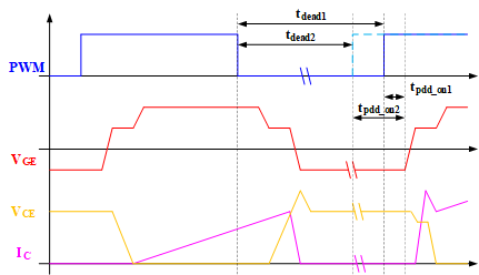
However, note that at least one TVS in the chain must be bidirectional, which can prevent reverse current flowing through the TVS during the forward recovery phase of the IGBT's reverse-parallel diode when it is in the on state. Such current would cause undervoltage in the secondary side power supply. As illustrated below, at the moment the diode turns on, its anode potential becomes significantly higher than its cathode for several hundred nanoseconds. During this process, the current path shown in the diagram below is formed. The path indicated by the red line represents a route of very low impedance, thereby enabling the generation of a substantial current. The current charges C3, thus raising the potential of VE. Consequently, the voltage between VE and VISO is reduced, which means the +15V voltage between VISO and VE is discharged. In practical applications, this process occurs periodically, synchronised with the switching frequency. Therefore, from a macro perspective, the +15V supply on the secondary side of the driver may experience dips. When this voltage falls below a predetermined threshold, the driver's undervoltage protection mechanism is triggered.
Firstack ASIC-based Driver advanced active clamping operation process:
Upon breakdown of the TVS by the Collector voltage, the current splits into two components: I1 and I2. I1 flows through the sampling resistor external to the ASIC, generating a voltage across it. The ASIC's internal comparator assesses whether to activate by comparing this voltage against a preset reference voltage: when the voltage across the resistor exceeds the threshold, the gate turn-off MOSFET is switched off, the turn-off current path is cut off, the gate is open circuit. I2 charges the gate capacitance, elevating the gate voltage VGE, and slows the turn-off current, thereby reducing the IGBT turn-off speed and achieving a voltage clamping effect.
3) Drive circuit
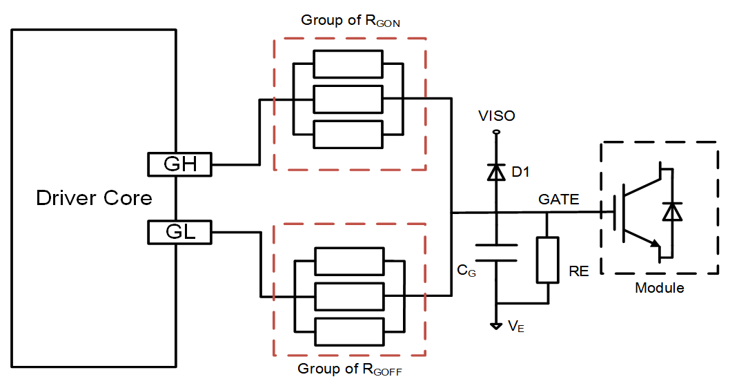
The driver connects a resistor to the IGBT gate via the gate drive terminal.
GH and GL pin control the turn-on and turn-off of the IGBT respectively, allowing separate turn-on and turn-off resistors to be set as required.
It is recommended to connect a resistor RE between GATE and COM (or VE).
In the event of driver power loss, this resistor provides a low-impedance path between the IGBT gate and emitter, preventing floating voltages from unintended IGBT turn-on.
Under IGBT short-circuit conditions, if excessive VGE voltage causes excessive short-circuit current, a clamping diode D1 may be added to the gate to clamp the gate voltage to VISO. Alternatively, a transient suppression diode may be connected between the gate and emitter. Schottky diodes must not be used as gate clamping diodes, and the breakdown voltage of the transient suppression diode must be considered.
Practical Exercise
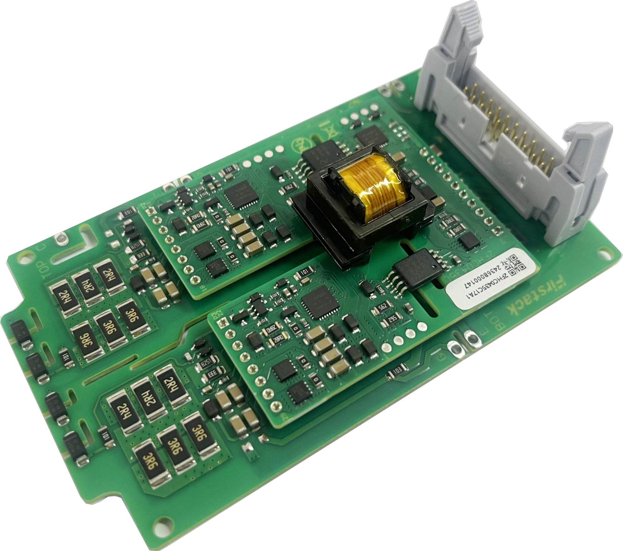
Taking the peripheral application circuit of the Firstack 2FHC0435C as an example:

I. Primary side peripheral circuitry
1. Fault pull-up circuit
The FAULT1 signal is routed from the core board and pulled up via a 4.7K resistor and diode.
Pull-up logic: High level indicates normal operation, low level indicates fault.
(The pull-up circuit may be implemented on the adaptor board/control board)
Furthermore, the Firstack driver supports intelligent fault management, where different faults correspond to distinct low-level durations, facilitating precise issue identification. Refer to the product manual for specifics.
(If using 5V PWM, pull-up to 5V)
2. PWM signal filtering circuit, ensuring signal input quality for more stable operation:
RC filter parameters may be adjusted according to practical requirements.
(If using 5V PWM, pull up to 5V)
II. Secondary side peripheral circuitry
1. The diode detection circuitry accommodates lower VCE, with the specific circuitry as follows:
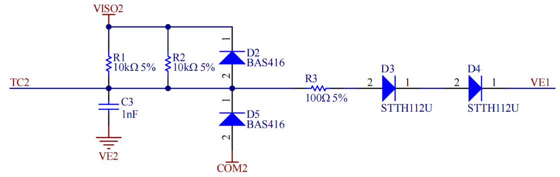
It should be noted that to prevent false fault alarms, the Firstack intelligent drive software incorporates a blanking period and filtering time, with a default fixed minimum duration of 4 μs.
2. Advanced active clamping based on ASIC
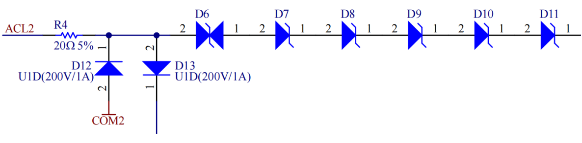
The diode (D13) requires feedback to the gate.
When the voltage across the left side of resistor R4 exceeds the set voltage, the driver initiates shutdown of the MOSFET;
and the performance of the active clamping can be enhanced by increasing the resistance value of the gate resistor Rgoff.
3. Drive circuit
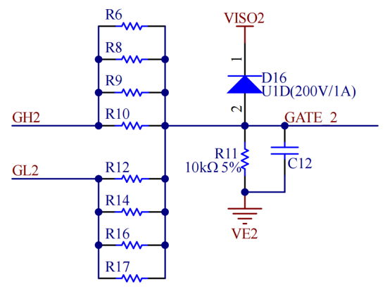
The driver connects a resistor to the IGBT gate via the gate drive terminal. The number of resistors connected in parallel is determined by practical considerations (such as PCB space, drive power requirements, etc.).
It is recommended that the R11 connected between GATE and COM (or VE) no less than 4.7kΩ.
In multi-parallel applications, the combined R11 must not be less than 4.7kΩ.
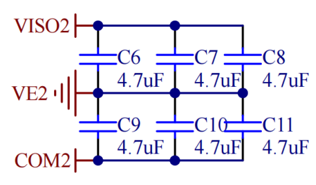
4. To ensure adequate drive capability, sufficient power supply support must also be provided
For IGBTs with gate charge within 3μC, the 2FHC0435 requires no additional capacitance on the secondary side for driving.
For IGBTs with higher gate charge, to guarantee stable logic levels during switching states, it is recommended to place appropriate support capacitors between VISOx-VEx and VEx-COMx respectively.
According to the corresponding IGBT specifications, when Qg exceeds 3μC, for each additional 1μC, the minimum capacitance between VISOx-VEx and VEx-COMx should be increased by 3μF respectively.
If the capacitance value exceed 150μF, please contact Firstack for technical support.
Notes
The content above provides a detailed breakdown of the matching board's principles and baseplate design, allowing selection based on practical requirements. However, for PCB design, the following considerations apply:
1. If the matched module exhibit a relatively high gate capacitance (Qg), it is advisable to incorporate additional capacitors on the baseplate to support the power supply. These capacitors should be positioned as close as possible to VISOx, VEx, and COMx to minimise parasitic inductance.
2. If the product fails to achieve the output power specified on the core board, pay attention to the gate resistor distribution! When driving excessive loads, gate resistors can generate significant heat. If positioned too densely or without additional cooling measures, this may impair the driver board's output power. Firstack recommends using through-hole resistors or surface-mount 2512 package resistors for gate resistors, supplemented by additional cooling methods including but not limited to:
1) Increasing the number of resistors in parallel
2) Increasing the layout spacing between gate resistors
3) Drilling holes on the PCB front surface
4) Creating windows on the PCB rear surface
5) Adding surface-mount copper strips to enhance heat dissipation.
3. Stress considerations during component placement: When designing adapter boards, pay attention to the orientation and distribution of resistors, capacitors, and other components. Account for stresses generated during application to prevent damage to components on the base board.
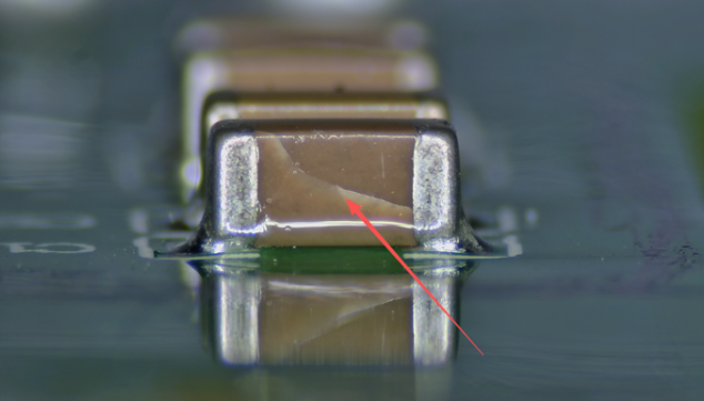
Capacitor cracking caused by failure to account for stress issues
If you wish to undertake in-house development, you may select the required functionalities based on the aforementioned specifications.
However, if you require a ready-made solution, please contact Firstack. We offer multiple tailored solutions.
ED single-switch product developed based on the 2FHC0435 – 2FHP0435EDL
Actual testing shows a single channel can achieve 3W at 50°C.

The figure above shows the measured temperature rise under ambient temperature of 30°C and a single-channel load of 3.8W.
- The 4FHP0435 series, a dual-parallel product based on the ED 2FHC0435.
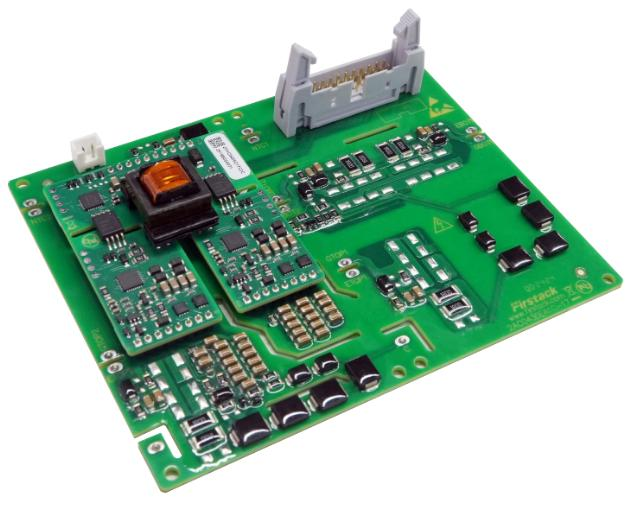
Available with two module centre distances (63mm and 82mm)
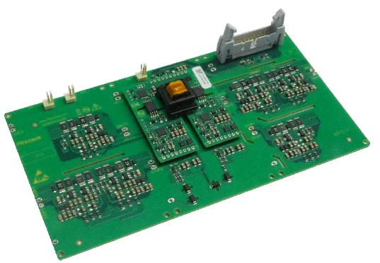
- ED triple-parallel product developed based on the 2FHC0435 – the 6FHP0435 series
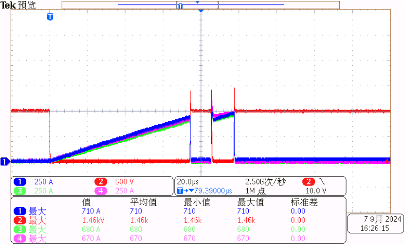
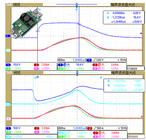
Current sharing waveform
Naturally, in addition to ED, we also offer solutions for Primepack encapsulation:
Developed based on the 2FHC0435 — the 2FHD0430C17.
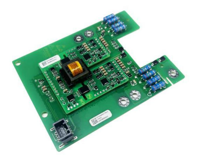
Compact structure with automotive-grade terminals, capable of delivering single-channel 4W at 60°C and 3W at 85°C for high-power drive applications.
If you require further product details or additional information, please do not hesitate to contact Firstack for more details.