In recent years, third-generation semiconductor technologies, exemplified by silicon carbide (SiC), have witnessed explosive growth. SiC MOSFETs are advancing from laboratory development to industrial production at an unprecedented pace. Leveraging their exceptional properties— high-frequency efficiency, low losses, and high-temperature resistance—they are accelerating the replacement of traditional silicon-based power devices in high-voltage applications such as electric vehicles, renewable energy systems, and industrial power supplies.
However, even the most formidable “muscles” require responsive “nerves” to command them. For SiC modules, a precise and reliable driver serves as this crucial “nervous system”. It connects to the control “brain” (the host computer), directing every action of the power “muscles” (the SiC modules). Should the driver malfunction, the entire system risks spiraling out of control.
Compared to the IGBT drivers we are all familiar with, what specific differences require our attention when designing drivers for SiC? How can we mitigate risks while fully leveraging its advantages? Drawing upon years of dedicated research and accumulated expertise, Firstack has distilled our practical insights from driver development into a series of specialized articles and will share with you in turn.
Miller Clamping
The first topic we shall explore is a crucial protective function in SiC drivers: Miller clamping.
To comprehend why it is indispensable and precisely how it functions, we must first examine a closely related phenomenon: bridge arm crosstalk. In a typical half-bridge circuit, the SiC MOSFETs in the upper and lower bridge arms (referred to hereafter as the ‘top switch’ and ‘bottom switch’ for clarity) turn on and off alternately. When the top switch is on, the bottom switch becomes its ‘opposite switch’, and vice versa. Then what constitutes bridge arm crosstalk? The crux lies in the Miller capacitance between the Gate (G) and Drain (D) of the opposite transistor. When the drain voltage of the opposite transistor undergoes a sudden change—such as a rapid rise in the bottom switch's drain voltage triggered by the top switch's conduction—a significant current flows through the Miller capacitance and is injected into the gate of the opposite switch. This abrupt current severely disrupts the stable turn-off voltage of the gate, causing its voltage to abnormally rise or fall. It may even reach the turn-on threshold or negative voltage limit, triggering unintended turn-on of the opposite switch or damaging its gate. The impact of bridge arm crosstalk on the gate is illustrated in the figure below:
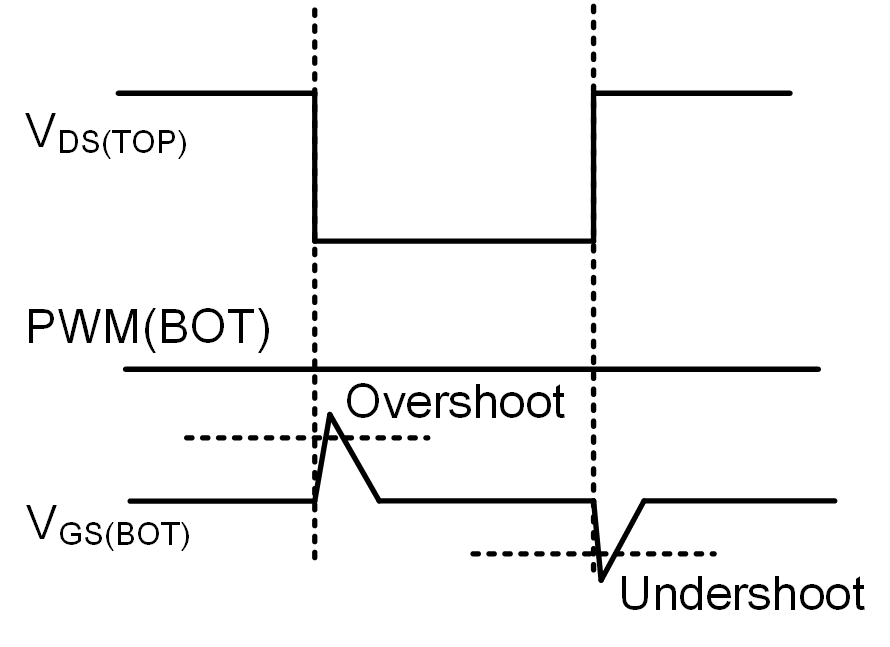
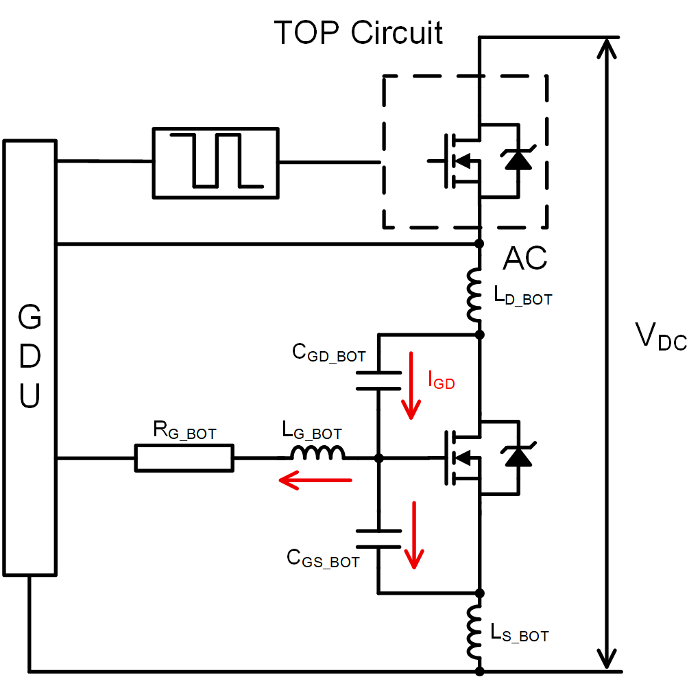
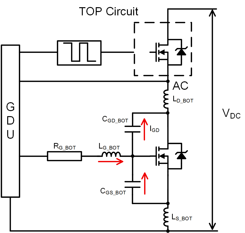
Take a specific scenario within a half-bridge circuit as an example: when the top switch (TOP) turns on, the voltage at AC rapidly rises from 0V to the bus voltage. In SiC devices, the rate of voltage change (dv/dt) during this process is exceptionally high, readily exceeding 10,000 V/μs. Such a dramatic voltage surge induces a significant current, Igd, through the gate-drain capacitance (Cgd) of the bottom switch (BOT) – commonly termed the Miller capacitance. This current injects into the bottom switch's gate, thereby elevating its gate voltage. Should this voltage exceed the device's turn-on threshold, it causes unintended conduction in the lower switch. This results in a direct connection between the upper and lower switch arms, inducing substantial short-circuit currents that may lead to overcurrent damage of the module. Similarly, during the top switch's turn-off process, the AC-side voltage rapidly drops from the bus voltage to 0V. At this point, a reverse Igd current is similarly coupled through Cgd, inducing a negative voltage at the bottom switch's gate. Should the absolute value of this negative voltage exceed the gate's withstand voltage threshold, it may directly damage the gate oxide layer, resulting in permanent device failure.
Based on the theoretical analysis, here is a set of actual double pulse test waveform, which can visually verify the effectiveness of Miller clamping. In this test, the driver's turn-off voltage was -6V.
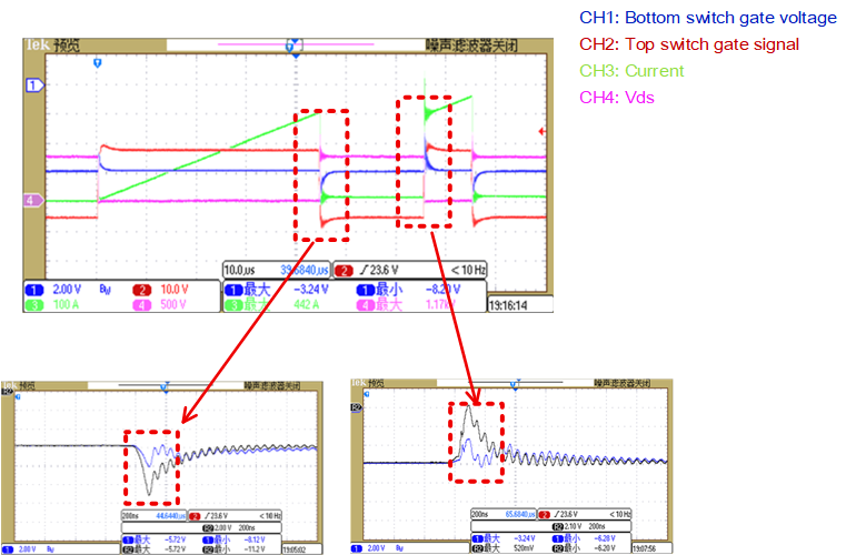
We conducted two sets of comparative tests: with Miller clamping enabled and another without Miller clamping, the waveforms were overlaid for analysis on an oscilloscope. We focused on observing two critical transient processes: the first turn-off and second turn-on of the top switch. It is clear that without Miller clamping, the gate voltage of the bottom switch exhibits significant positive peaks and negative dips, whereas with Miller clamping, the voltage remains relatively stable throughout.
The test data aligns perfectly with prior theoretical analysis: upon turn-off of the top switch, the gate of bottom switch, which is without Miller clamping, experienced negative voltage overshoot, dropping to -11.2V. Upon turn-on of the bottom switch, its lower gate experiences a positive voltage overshoot, lifting the voltage to 0.52V. Owing to the presence of parasitic inductance within the power circuit, there’s oscillations are in the subsequent waveform.
However, a crucial factor remains unaccounted for in the above analysis: the influence of the gate-source capacitance (Cgs) upon the gate voltage. In fact, during rapid changes in gate voltage, a coupled current Igs also flows through Cgs. To more precisely analyse the overall situation during positive voltage overshoot, we may equate the gate circuit to the following circuit and derive the corresponding formula:
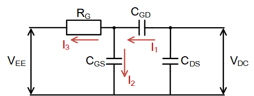
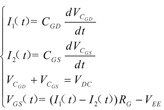
As dv/dt approaches infinity, solving the equation yields an approximate value for Vgs:
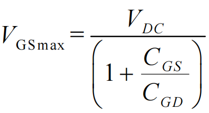
Based on the above formula, the maximum negative overshoot of Vgs can similarly be derived (take the negative value of the formula). The analysis clearly reveals a crucial relationship: the magnitude of voltage overshoot is inversely proportional to Cgs. In other words, increasing the capacitance value of Cgs is a direct method of suppressing overshoot. However, this approach comes at a significant cost—increasing Cgs substantially elevates gate charge, thereby slowing switching speed and increasing switching losses. This directly contradicts the core advantages of SiC modules: high frequency and high efficiency. Consequently, in engineering design, suppressing overshoot by simply increasing gate capacitance is not recommended.
In summary, Miller clamping plays a crucial role in high-voltage, high-speed switching transients. Its core mission is to fundamentally safeguard system reliability and operational efficiency by real-time suppression of both positive gate voltage rise (preventing false turn-on) and negative overshoot (preventing gate damage) caused by arm crosstalk. Then what lies at the heart of the design that can achieve this critical function? The answer is clear and direct: by establishing an additional, independent, rapid, low-impedance discharge path for interference currents, thereby firmly clamping the gate voltage within a safe, stable range.
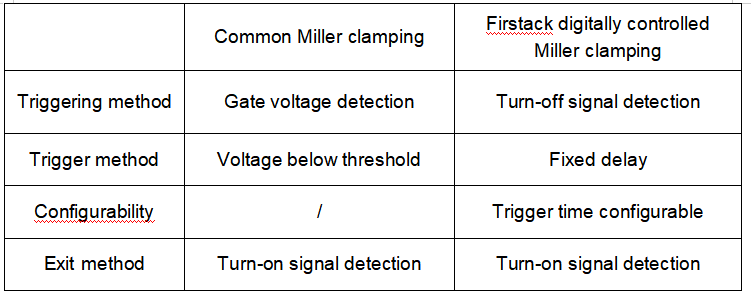
Currently, all SiC drivers from Firstack are developed based on the new digital ASIC platform and come standard with digitally controlled Miller clamping, which provides a robust guarantee for system robustness and high efficiency at the hardware level. Firstack digitally controlled Miller clamping solution achieves remarkable hardware simplicity, as illustrated below. The functionality is realized by a single independently controlled MOSFET, with the control signal sourced directly from Firstack digital ASIC.
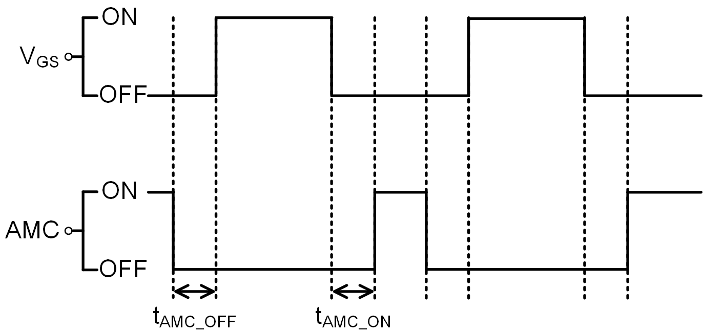
Compared to common solutions on the market, the number of components is reduced by up to 80%. This not only significantly enhances integration but also reduces potential failure rates at source, markedly improving system reliability. At the intelligent control level, this technology likewise demonstrates outstanding advantages. Based on shutdown signal detection and employing a fixed delay (tAMC_ON) trigger mechanism, it can precisely distinguish between normal switching actions and harmful signal interference, fundamentally eliminate false triggering caused by gate voltage fluctuations, ensuring the accuracy and reliability of protective actions. The diagram below illustrates the specific timing logic for the digital Miller clamping.
Moreover, its programmable parameter characteristics overcome the inherent limitations of traditional hardware solutions. Users can flexibly configure parameters according to specific device characteristics and system operating conditions, effortlessly addressing highly customized application scenarios and achieving precise optimization of system performance.
Besides Miller clamping, there are other methods to mitigate the effects of gate crosstalk, such as increasing the capacitance between the gate and source, altering the gate resistance, adding a common-source inductor to the gate and so on, we shall not elaborate further here.
It should also be noted that in conventional IGBT driver design, reliable device turn-off is typically achieved solely through negative voltage turn-off, without dedicated Miller clamping. However, with technological advancements, the switching dv/dt of certain high-speed IGBTs currently available on the market approaches 10,000 V/μs. In such high-voltage, high-speed applications, empirical evidence indicates that the risk of false conduction induced by arm crosstalk can no longer be disregarded. Consequently, even for IGBTs, incorporating Miller clamping into their drivers based on test results is increasingly becoming a necessary design consideration to enhance system robustness.
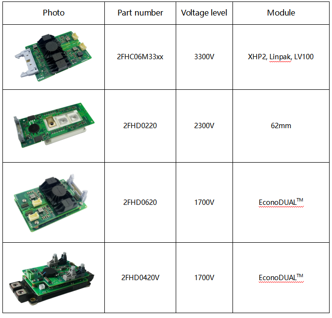
The following table lists the SiC driver models currently equipped with the latest ASIC platform and their descriptions:
For further information, please contact Firstack, our professional team will assist you with product selection and any necessary technical discussions.