Introduction
There are three types of solutions: resistance schemes, resistance-capacitance (RC) schemes, and active clamping schemes due to the voltage imbalance issue in 3L-ANPC converters. These schemes can achieve voltage balance sharing both statically and dynamically, each with its own advantages and drawback. The resistance scheme is relatively simple and low in cost; selecting a large resistor can balance the steady-state voltage balance (during standby and shutdown), while selecting a small resistor will result in high power consumption of the resistor. Inappropriate parameter selection for the resistance-capacitance (RC) scheme may easily cause wrong waveform of the bridge arm. For the active clamping scheme, there are issues related to the precision of the TVS devices used and their power consumption.
Keyword:3L-ANPC; resistance schemes; resistance-capacitance (RC) schemes; active clamping schemes
Abstract
Although there is voltage imbalance in the 3L-ANPC system, it is currently the preferred topology for inverter solutions due to the use of low-voltage devices to achieve high DC voltage. By designing the GDU and power module, voltage imbalance can be optimized. Chapter 1 mainly analysis the mechanism of voltage imbalance inside and outside the 3L-ANPC switches; In Chapter 2, the suppression of internal switches over-voltage is achieved by investigating resistance methods, resistance capacitance RC schemes, and active clamping methods. Simultaneously analysis the advantages and drawback of the above three schemes, and figure out which method to use based on different working conditions in practical engineering applications.
1.1 Resistance Schemes
As shown in the figure below, add a resistor Rs between C in T2 and E in T3. This method is a simple way to suppress voltage imbalance between the inner and outer switches. The addition of resistor Rs adds two paths (one for the positive and one for the negative half cycles). According to the conclusion of Chapter 1, over-voltage occurs when the output potential (AC) changes from O to P/N. The following figure analyzes the working state of 3L ANPC according to i>0. From the continuous current state of D5/T6 (T1--T4 corresponds to 0-1-1-0) to T1 turn-on (T1--T4 corresponds to 0-1-1-0), resistor Rs is connected to VP through T1. If the voltage of T3 is higher than VDC/2, the D6 diode will operate and the voltage of T4 will always be VDC/2; If the voltage of T4 is lower than VDC/2, Vbus+ charges the IGBT junction capacitor Ct4 of T4 through T1 and Rs until the voltage reaches VDC/2 and D6 conducts.
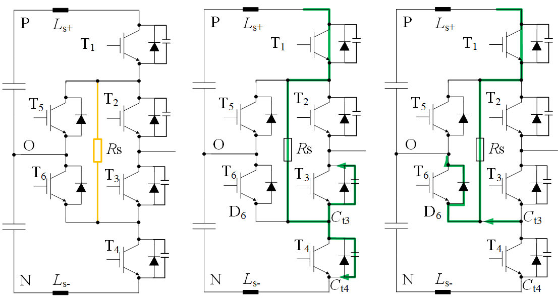
Rs Position of equalizing resistor Rs Charging D6 Turn-on
Fig.1 Rs Voltage Balance Principle
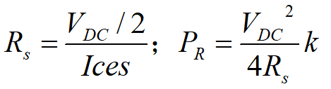
When the inverter is in operation, T1 and D6 conduct Rs resistance to withstand VDC/2 or T4 and D5 conduct Rs resistance to withstand -VDC/2, that is, Rs resistance is always VDC/2. There is dissipated power on the Rs resistor. The voltage equation (KVL) when T3 and T4 are turned off is:
Among them, Vspike(0+) is the voltage generated by parasitic inductance, and Vcet3, Vcet4 are the terminal voltages of IGBT. Due to the effect of Rs, the maximum voltage of T4 is VDC/2, so the T3 voltage is:
If the inverter is in standby or shutdown and Vspike(0+)=0, the T3 terminal voltage will always be ≤VDC/2. If it is in operation, Vspike(0+)≠0。 Through dual pulse testing, the IGBT driver selects appropriate gate level parameters to control the T3 voltage within the SOA safe working area of the IGBT.
How to choose the parameters of Rs?
If the design goal is to achieve equal voltage distribution between the inner and outer tubes of the inverter during steady states such as standby and shutdown, selecting a larger Rs resistor is beneficial for reducing power consumption and improving efficiency. The following formula can be used for selection:
In formula above, Ices is the leakage current parameter of IGBT. If a 1200V IGBT is used, the Ices leakage current parameter at a cut-off voltage of 1200V can be found in the specification data sheet, generally between 0.1mA-10mA; k is usually selected as 4-5 for the power margin of the resistor; As mentioned above, the resistance of Rs for a 1500V DC system is between 7.5MΩ and 750kΩ.
If the design goal is for the inverter to be able to evenly do voltage balance during dynamic operation, it is necessary to consider parameters such as the system's switching frequency, minimum duty cycle, IGBT junction capacitance, etc., so that the T3 junction capacitance can be charged to VDC/2 within the minimum duty cycle of the system. The disadvantage is that the Rs resistance is small and the power consumption is high. At this point, Rs charges the junction capacitor to satisfy the first-order circuit full response formula:
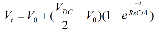
Among them, Vt is the time-domain voltage of T3 capacitor, and V0 is the initial voltage of T3 (the initial voltage is distributed by T3 and T4). At present, testing methods cannot accurately measure this voltage (by clamping the probe, increasing impedance, and voltage changes). The higher the initial voltage, the smaller the resistance of Rs. It can be estimated that V0=VDC/4. By substituting formula above, three time constants can be obtained to achieve VDC/2.
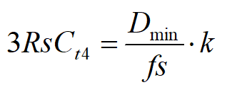
Among them, Dmin is the minimum duty cycle, fs is the system switching frequency, and k is the coefficient (RC needs to complete charging T3 within a certain time while not exceeding the pulse width time corresponding to the minimum duty cycle of the system). For a 1500V high-power system with a switching frequency of 3kHz, a minimum duty cycle of 5%, an IGBT junction capacitance of 10nF, and k=50% (minimum pulse width time of 50%), the Rs resistance is calculated to be 275Ω, and the dissipated power is 2kW, requiring the use of a resistor with 8kW power. If using a 1500V commercial storage and string system with a switching frequency between 12kHz-16kHz, a smaller Rs resistor is required to suppress dynamic voltage balance.
As mentioned above, the Rs resistor scheme can effectively address steady-state, standby, and shutdown conditions by selecting a large resistor. If we want to suppress the dynamic voltage imbalance in each switching cycle, we need to use small resistors, which consume more power and reduce the efficiency of the inverter. At the same time, the resistance scheme can only clamp the T4 voltage to VDC/2, and the over-voltage of T3 (Formula 2) needs to be controlled within the SOA through dual pulse testing combined with IGBT driver parameters. Due to considerations of resistor power consumption, selection, and system efficiency, larger resistors are generally chosen.
1.2 Improved Resistor Scheme
As shown in the figure below, connect a single Rs resistor in parallel across T2 and T3, so that the voltage between T2 and T3 is equal to the voltage across the resistor. In steady state, there is also a voltage imbalance between T2 and T3. Therefore, the Rs resistor can be split in half into Rs1 and Rs2, which further equalizes the voltage of T2 and T3 while retaining the original characteristics of the resistor scheme.
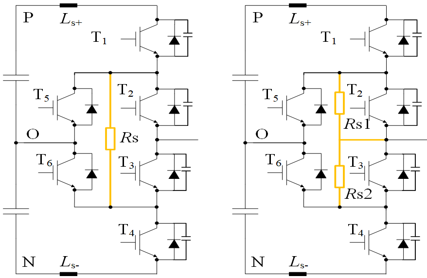
Fig.2 Improved Resistor Scheme
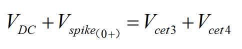
2.1 Resistance-capacitance (RC) Scheme
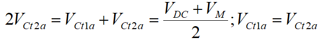
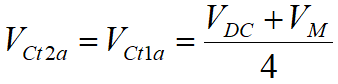
As explained in Chapter 1, the reason for the impact on voltage balance is due to the different junction capacitors of the 3L-ANPC topology charging circuit, where the charging current flowing through the inner switches junction capacitor is greater than the voltage imbalance caused by the outer switches current. If capacitors C3 and C2 (compensating capacitors) are connected in parallel to T3 and T2 IGBTs respectively, the voltage can be reset. The basic principle is to increase the equivalent capacitance of the inner switches by compensating the capacitor to make it the same as the equivalent capacitance of the outer switches, so that the voltage of the inner and outer switches can be balanced during charging and discharging. Simultaneously, a resistor Rc is connected in series with the C3 and C2 capacitors to limit the current surge of the compensating capacitor on the IGBT. Formulas in Chapter 1 can be rewritten as follows:
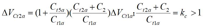
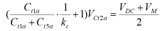
As shown above, if the selected C3 capacitor is exactly equal to the IGBT junction capacitor, and T1、T5、T2 are modules of the same model, Ct1a=Ct2a=Ct5a=C3。 T1 and T2 have the same voltage to achieve voltage balance.
For MW level inverters, high-power IGBT modules with junction capacitance between 5nF-20nF are used. The IGBT CE junction capacitance is equal to the output capacitance minus the input capacitance (which can be obtained through semiconductor manufacturers). At the same time, the selection of C3 and C2 capacitors can also be greater than the IGBT junction capacitor, which can be considered from the aspects of actual measurement effect and loss. The selection of resistor Rc can be based on formula 5. The power consumed by the charging and discharging energy of the capacitor falls on resistor Rc and the resistor power is calculated as follows:
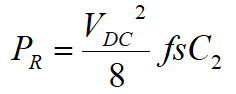
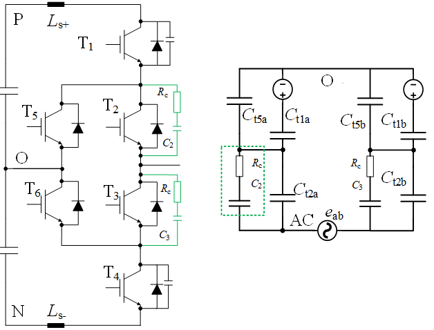
Fig.3 Resistance-capacitance (RC) Equivalence Principle
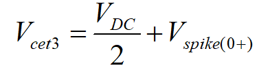
2.2 Improved RC scheme
For kW level inverters, PCBA is usually used as the power circuit. According to the introduction in 2.1, high-voltage resistors and capacitors can be arranged in series or parallel on the PCB. However, for MW level converters, high-power IGBT modules and stacked copper bars are usually used without PCB, so a set of RC is used for high-power implementation. Connect resistor Cs in series with the balanced resistor introduced in section 1.1. The advantage of the improved RC scheme is that it reduces a set of resistors and capacitors, but the disadvantage is that the power consumption of Rs has doubled. Power resistors and capacitors can be used in high-power applications.
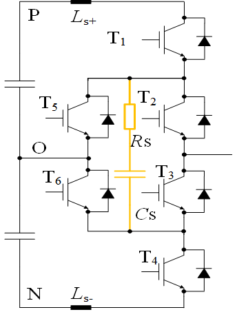
Fig.4 Improved RC scheme
As mentioned above, the RC scheme allows energy to be fed back to the system due to the presence of C, while also reducing the power consumption of the R resistor (compared to pure resistors). At the same time, capacitors also have a voltage clamping effect (voltage cannot suddenly change). For kW level converters, dual RC can be used, while for MW level converters, single RC can be used. Due to over-voltage caused by circuit inductance, it can only be controlled within the IGBT SOA range through a dual pulse testing scheme in conjunction with IGBT drivers. At the same time, in response to the LC resonance of the current during shutdown, adopting the RC scheme can increase the damping coefficient of the second-order circuit, reduce the oscillation angular frequency, and accelerate convergence.
3.1 Active Clamping Scheme
The goal of an active clamp circuit is to clamp the IGBT collector voltage so that it does not become too high. This function is mainly used when the IGBT turn off voltage is too high due to abnormal operating conditions of the inverter, and the circuit does not work normally. This circuit consists of TVS tubes and fast recovery diodes. When the collector current of IGBT is too high, TVS is broken down, and current flows into the gate, causing the gate potential to rise, thereby reducing the turn off speed and decreasing the peak. Its essence is a negative feedback loop, with the controlled object being the IGBT collector voltage. As shown in Fig.5, when the collector voltage of IGBT exceeds Vz, the TVS is absorbed by the energy of the breakdown voltage spike, and the current Iz flowing through the TVS simultaneously generates dissipated power consumption. The circuit of this active clamp scheme is relatively simple, but there are the following problems: 1) The breakdown voltage of TVS devices has individual dispersion and accuracy issues, generally 5-15%, and there is a problem of voltage consistency after batch use. 2) As shown in Figure 6, TVS experiences a rapid increase in Vz voltage at different current and voltage levels. When the current exceeds the operating voltage Iz1 and reaches the operating point Iz2, the overall clamping voltage Vz increases. 3) In response to the unbalanced voltage inside the 3L-ANPC switches, this circuit is more effective for dynamic voltage. If there is long-term uneven voltage during standby and shutdown, the TVS will continue to operate, resulting in high power consumption and heating failure. 4) Regarding the current widespread use of three-level multi parallel scheme in MW level inverters, if active clamps are added to each parallel path, the actual engineering effect needs to be verified:
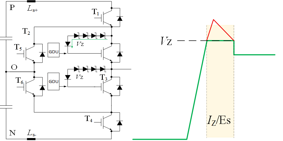
Fig.5 Active Clamping Scheme
Fig.6 TVS Characteristic Curve
Regarding the above issues, scholars and engineers have proposed some improvement measures. As shown in Fig.7a), a current loop is added on the basis of Figure 5 to turn off the low impedance state Boost, thereby reducing the TVS current and power consumption to control the clamp Vz voltage. The problem with this circuit is that the Boost action takes time, increasing the response and phase delay of the clamp circuit. As shown in Fig.7b), a switching device is used to bypass Vz2. When the IGBT turn off voltage is higher than Vz1, TVS will operate to cut off the switch and put VZ2+VZ1 into operation. Because VZ1 cannot operate frequently, the two-stage voltage requires VZ2 to use a lower threshold. In the dual pulse testing, it is necessary to control the peak voltage of the inner tube to be lower and increase the inner tube loss. At the same time, it cannot solve the problem of long-term power consumption in steady state. Fig.7c) shows b) a low-cost solution that utilizes capacitive characteristics for short-term bypass TVS.
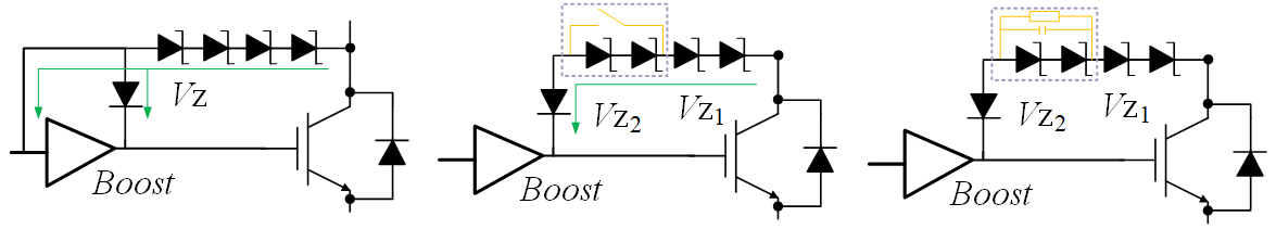
a) Advanced Clamping b) Switch Type Dynamic Clamp c) RC Dynamic Clamp
Fig.7 Improved Active Clamping
As mentioned above, the active clamping scheme is beneficial for dynamic voltage, but for static voltage, there may be continuous power consumption that easily exceeds the device's heat capacity, leading to device failure. Even adding dynamic clamping can not solve static problems, and it will also increase the loss of the inner switches switch. For power schemes with small parasitic inductance (such as the Easy series), low turn off voltage, and large voltage margin, when there is enough space to place multiple TVS, it can be attempted (actual effect will be determined through testing). For multi-level and multi parallel schemes, standard half bridge modules (such as ED3 and PP3) are usually used in combination, with parasitic inductance typically ranging from 100nH to 250nH, high turn off voltage, and difficulty in setting the active clamp threshold voltage.
Summary
From Chapter 1, it can be concluded that the main reasons of imbalance are circuit stray inductance, IGBT parasitic capacitance, etc. Based on the actual situation of engineering applications, the summary is as follows:
(1)The parasitic inductance in the power module is large and the stored energy is high: optimize
the circuit inductance.
(2) The discreteness of module junction capacitance, especially the random allocation of T5T6 to
large junction capacitance modules: single bridge arm module matching.
(3) Adding midpoint balance control to the three-level system leads to asymmetric IGBT switching actions in the positive and negative half cycles: optimize the control method or increase the DC capacitor.
(4) IGBT itself has switching characteristics such as dv/dt, fast speed, and strong excitation source: adjust the speed appropriately.
The three solutions introduced in Chapter 2 cannot simultaneously solve problems such as standby, shutdown current oscillation, and voltage imbalance during operation, nor can they solve the problem of over-voltage caused by internal switches shutdown. Therefore, after the module design is completed, it is necessary to conduct dual pulse testing with IGBT drivers to obtain and debug the appropriate dv/dt and turn off over-voltage, and balance the inner switches voltage with the above three methods. The Firstack driver identified this issue as early as 2018 and integrated a balancing resistor (as shown in Figure 2) on the ED series driver to balance the voltage during standby and shutdown (steady state). Firstack's IGBT/SiC design concept based on system thinking can effectively identify pain points and problems in power modules, and optimize the design through driving design.
*Due to the limited level of the author, please point out any shortcomings. Thank you.
Reference
[1].张兴.《PWM整流器及其控制》,机械工业出版社,[M].
[2].林渭勋.《现代电力电子技术》,机械工业出版社,[M].
[3].Ting Lu.et al.Parameter Design of a Three-Level Converter,[C].
[4].网络资料