Abstract
3L-ANPC are connected in series with two low-voltage components to increase the DC voltage of the system, which cause an imbalance in the voltage between the inner and outer switches easily in real system, causing the inner switches voltage to exceed half the bus voltage, posing a threat to system operation. In response to this issue, this article analysis the mechanism of voltage imbalance between the inner and outer switches of the 3L-ANPC grid connected system under normal operation, grid standby, and fault shutdown conditions. The main reasons for the voltage imbalance problem are the stray inductance of components in the circuit, asymmetric charging and discharging of inner and outer switches junction capacitors, and circuit oscillation. Feasibility analysis of solutions for voltage imbalance inner and outer switches simultaneously.
Key words: 3L-ANPC; inner and outer switches; voltage imbalance; parameters; charging current
Introduction
With the gradual increase in grid connected voltage levels of new energy generation systems, 3L-ANPC has the advantage of using low-voltage components to reach high-voltage systems and is widely used in medium to high power converter systems. Due to the distribution parameters of the circuit and components, voltage imbalance may occur during the operation of a three-level inverter, causing the inner switches voltage to exceed half of the bus voltage, or even exceed the inner switches components voltage. High power inverter systems typically use IGBT devices, as IGBT is a voltage sensitive device and over-voltage can cause device failure. Based on actual working situation, analyze the mechanism of voltage imbalance inside and outside the 3L-ANPC system under typical working conditions such as grid connected standby, normal operation, and fault shutdown, and provide corresponding solutions. Through GDU and module design, which can be used to reduce or suppress uneven voltage conditions.
This article is divided into two chapters. Chapter 1 mainly investigate the mechanism of voltage imbalance inner and outer the 3L-ANPC switches; Chapter 2: Analysis solutions to voltage imbalance from the perspectives of GDU and modules
1. 3L-ANPC Mechanism of voltage imbalance between inner and outer switches of IGBT devices
1.1 Voltage imbalance between inner and outer switches under standby conditions
When the inverter is in standby mode, all IGBTs are turned off, and the voltage on them mainly depends on the charging and discharging process of the junction capacitance, only considering the distributed capacitance in the power unit, as shown in the following figure. C1、C2 are the upper and lower half cycle capacitors, VDC is the total DC voltage; Ct1a--Ct6a is the junction capacitance corresponding to the A-bridge arm IGBT; Ct1b--Ct6b is the junction capacitance corresponding to the B-bridge arm IGBT; iCt1a, iCt2a, iCt5a are the currents flowing through Ct1a, Ct2a, Ct5a, respectively.
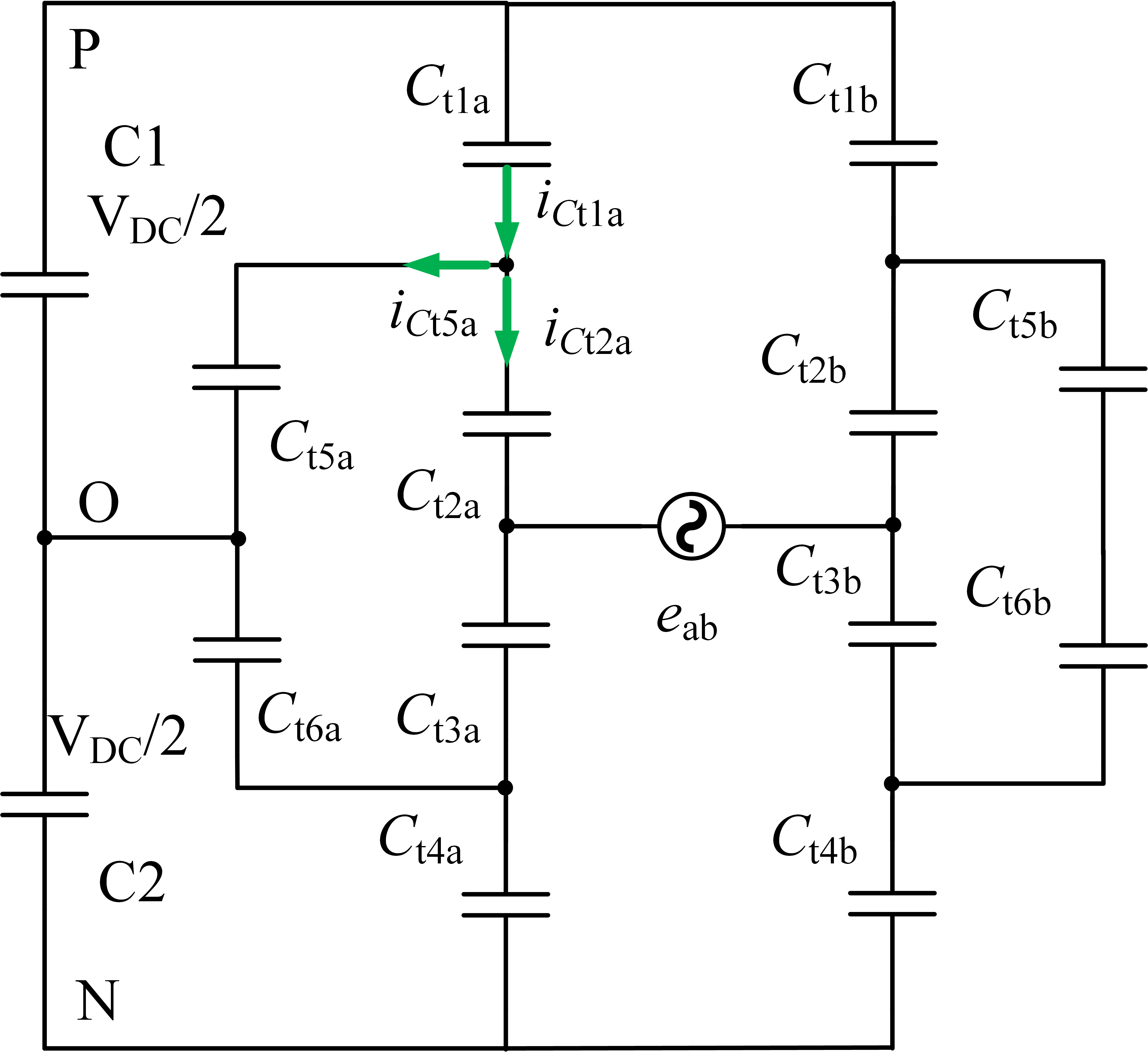
Fig.1 Equivalent circuit diagram under standby condition
Since the half bus voltage remains constant, the bus voltage can be considered as a constant voltage source, as shown in the figure:
Then:
Then:
According to KCL:
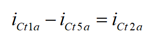
Due to formula above:
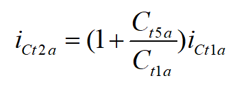
Since T1 and T2 use the same type of IGBT, so Ct1a=Ct2a,and formula of voltage:
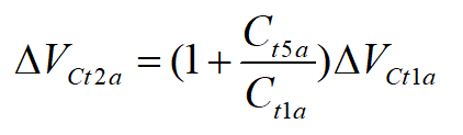
In the above formula, VCt1a, VCt2a, VCt5a are the corresponding voltages on phase A T1, T2, T5; If VCt3b, VCt4b are the corresponding voltages on B-phase T3, T4; According to the KVL theorem, there are:
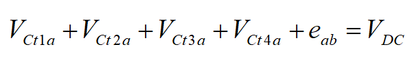
Among them, eab is the grid connected voltage of phase ab, eab(t)=VMsin(ωt+θ), and the maximum value of VM grid connected voltage. When the voltage of the eab power grid changes from VM to -VM, VCt1a, VCt2a, VCt3b, VCt4b continuously increase whileVCt1a+VCt2a=VCt3b+VCt4b; When eab=-VM, the voltage reaches its maximum value VDC+VM. Combining formula above, it can be concluded that:
Usually, T1, T2, T6 choose IGBT modules of the same model, so the corresponding Ct1a=Ct5a; For an energy storage system with a DC 1500V three-level and an AC output effective value of 690V, according to formula above, VCt2a=825V (the lowest withstand voltage of the selected device); For wind power converters with DC 1800V three-level and AC output effective value of 1140V, VCt2a=1137V; Considering the impact of cosmic ray FIT on IGBT, a 1.2-1.5 margin should be reserved for the selected IGBT withstand voltage. Typically, energy storage systems use 1200V devices, while wind power systems use 1700V devices.
If T5 chooses different types of IGBT modules, if Ct5a>Ct1a, the resulting VCt2a is higher and requires IGBT with higher withstand voltage. Therefore, when using a hybrid module, the smaller the junction capacitance of T5 (T6) module, the safer it is.
1.2 Voltage imbalance under normal operating conditions
When the grid connected inverter works during normal operation, there are three working states of AC output voltage (P, O, N); There are two states of AC current: i>0, i<0. This article analyzes the working state of 3L ANPC according to i>0, and since the output inductor current can not suddenly change, the inductor is investigated according to the current source.
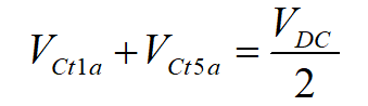
As shown in the figure below, the output is O voltage, and current flows through D5 and T2; When T1 is turned on, the current flowing through T1 increases. If the current is less than the load current IL, D5 will conduct normally, and the output voltage at this time is still O. When T1 current rises to IL, D5 will turn off, and after reverse recovery time, it will completely turn off, and the output voltage is P. T3 and T4 are subjected to the full bus line voltage VDC. Due to the presence of inductance Ls+, current will continue to flow out, charging the T3 junction capacitor, making the voltage of T3 greater than VDC/2. If the charging time and current are large (Ls+ stores more energy), T3 may be over-voltage.
O Condition T1 Turn-on T3 Over-voltage
Fig.2 O→P Conditions
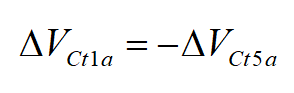
The following figure shows the process of P to O. The initial voltage is in the P state and is switched through T1, T5, T6. After T1 is turned off, the voltage of T1 continues to rise, the current decreases, and the output voltage decreases. When the current of T1 is less than IL, D5 and T6 conduct and flow current. T3 and T4 are subjected to VDC/2 voltage. Due to the conduction of T3, the voltage of the T3 junction capacitor continuously decreases and eventually reaches 0. That is to say, there will be no over-voltage situation in T3. The final voltage of the T4 junction capacitor charging will reach VDC/2.
P condition T1 Turn-off (time) T3Turn-on
Fig.3 P→O Condition
As mentioned above, when switching from O to P or N in a three-level converter, it is easy to cause voltage imbalance in the inner switches, with the inner switches voltage being relatively high, exceeding VDC/2; When switching from P or N to O, there will be no over-voltage situation; The main reason for the above phenomenon is that the energy of stray inductance in the circuit is transferred to the inner switches junction capacitor during the commutation process.
1.3 Analysis under shutdown conditions
3L-ANPC needs to follow the inner and outer switches shutdown sequence when shutting down, that is, the outer switches should be turned off first, and then the inner switches should be turned off. The following diagram shows the shutdown schematic when the current i>0 and the output voltage P are reached.
The output voltage is P, and T1 and T2 are conducting, in the initial state. At this time, T1 is turned off, D5 and T6 enter the freewheeling state, and the output voltage is O. After T2 is turned off, the freewheeling path switches to D3 and D4, and the output voltage is N (before T6 is turned off, the output is O, and the final state T6 will hang up, and the output voltage is N). After the continuation of D3 and D4, the output current i is not directly 0A, there will be an oscillation process, during which there is a state of i<0, that is, the current flows into the bridge arm.
At this time, discharge Ct1, Ct2, while charging Ct3, Ct4. Due to the existence of two charging paths in Ct3, the charging speed is faster than that of Ct4. After the final charging and discharging are completed, the current i flows through D1 and D2, and the output voltage is P. At this time, the voltage of T3, which charges faster, is higher than VDC/2. If it exceeds the safe working area of IGBT, there may be over-voltage risk.
Fig.4 Status during downtime
Perform equivalent circuit model analysis on the above circuit, as shown in the following figure: Ls is the equivalent inductance of the circuit for stray inductance, R is the equivalent resistance of the circuit, Ct1--Ct6 is the equivalent junction capacitance of IGBT corresponding to T1--T6. Since C1 and C2 are DC capacitors of the inverter, the capacitance value is large enough, so a constant voltage source can be used to indicate a voltage of VDC/2. As analysis above, after the continuous current of D3, D4 is completed, current i charges the 6 junction capacitors. Due to Ct1=Ct4, Ct2=Ct3, Ct5=Ct6 (symmetrical parameters of the upper and lower bridge arms), it2=i/2. At the same time, the charging current of it2 is the highest (it2>it5, it2>it1), and the voltage of T2 switches is the highest. Therefore, in the shutdown state, the voltage of the inner switches is also higher than that of the outer switches. At this time, Ct1, Ct2 are in a discharge state. When the voltage of Ct1, Ct2 is 0V, the current i flows through D1 and D2. When the current i decays to 0A, it enters a reverse oscillation with i<0, discharging Ct3, Ct4 and charging Ct1, Ct2. This cycle continues. This process is related to the oscillation frequency and amplitude during current shutdown.
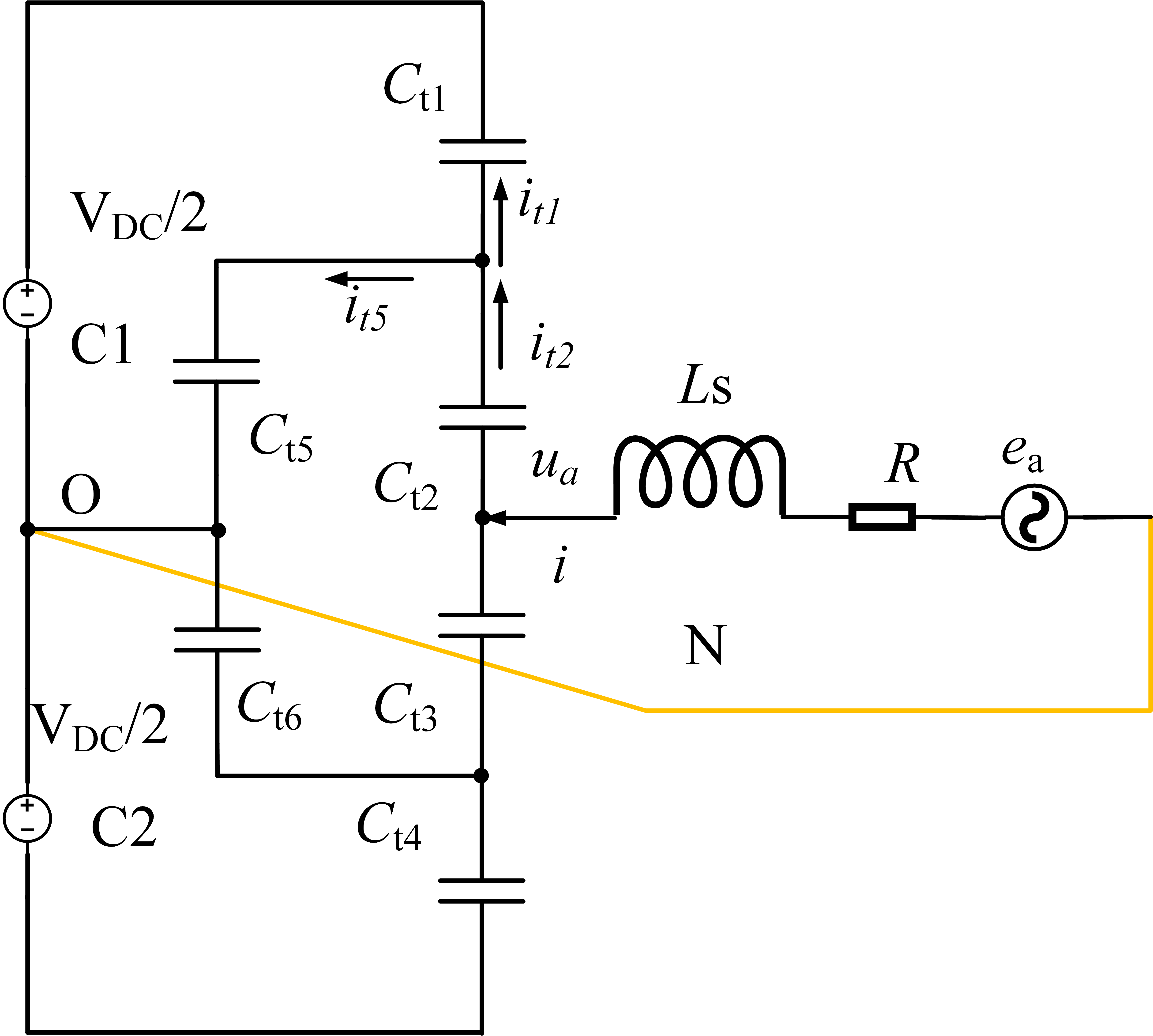
Fig.5 Equivalent circuit for charging and discharging after shutdown
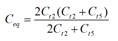
The circuit equation can be established through the above equivalent circuit. The Ct1--Ct6 capacitor and the two constant voltage sources C1 and C2 can be analysis using the Thevenin equivalent principle to obtain the following circuit model. The above junction capacitors Ct1--Ct6 can be equivalent to Ceq,
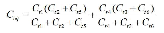
In formula above, Ct1=Ct4, Ct2=Ct3,Ct5=Ct6; If T1, T2, T3, and T4 choose the same components, formula above can be simplified as:
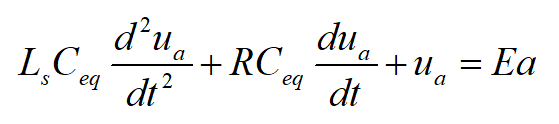
As investigation above, after T2 shutdown, D3/D4 continuation, and current reverse oscillation, the AC point will exhibit three states N, O, and P. Assuming the initial state is N (VDC/2), the process from N to P is the process of AC point voltage from - VDC/2, 0, VDC/2, where Ea is the grid excitation and R is the resistance of the circuit. The corresponding is the LRC second-order oscillation circuit.
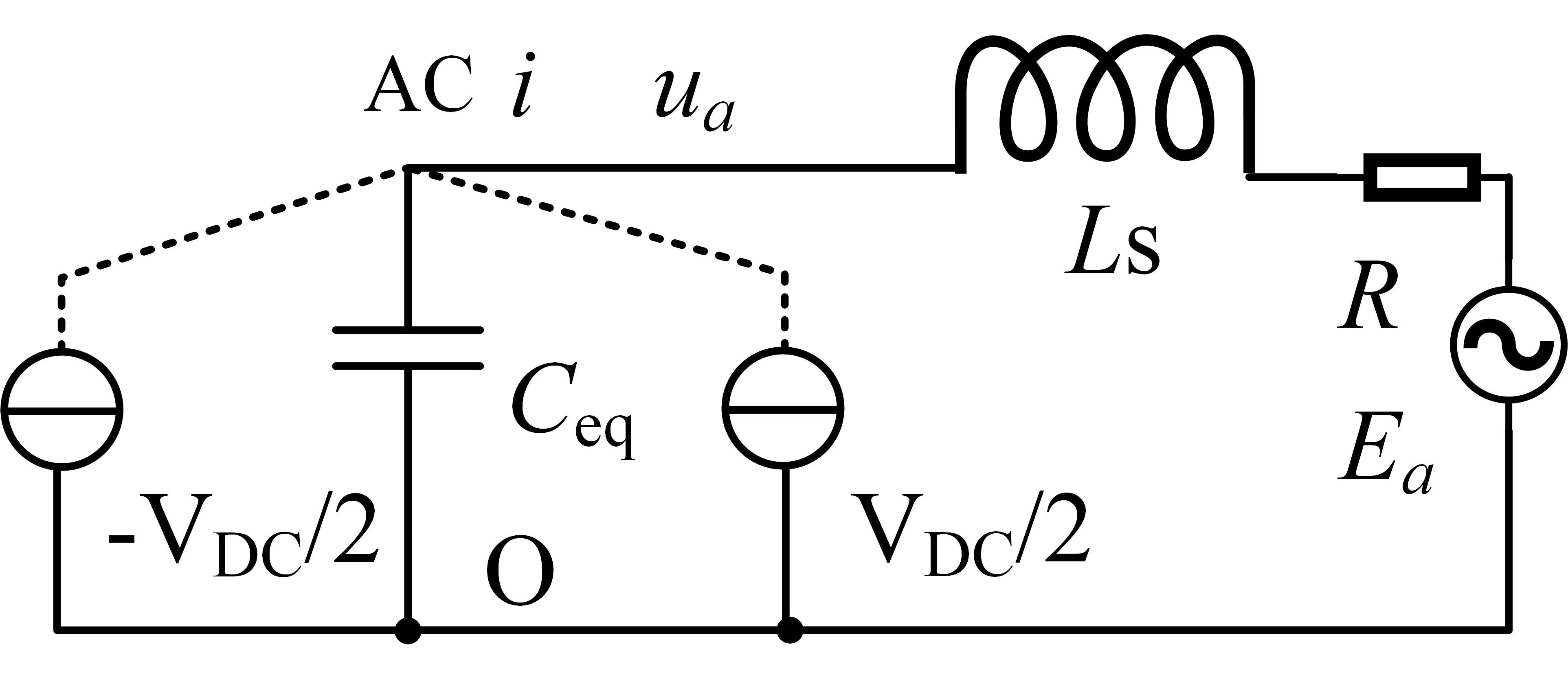
Fig.6 Second-order LRC
This process can be seen as the excitation of the circuit (related to amplitude and frequency). The following circuit is a second-order circuit, and the circuit equation is as follows:
Damping coefficient, resonant angular frequency, attenuation coefficient
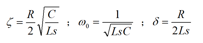
The larger the attenuation coefficient , the faster the attenuation. In high-power 3L-ANPC systems, the resistance R corresponding to the bus bar is usually smaller, but the inductance Ls is larger. Easy to experience under damped oscillations during shutdown. The specific parameters of LRC can be obtained through finite element simulation and calculated by combining the junction capacitance parameters of IGBT.
In summary, the mechanism of voltage imbalance between the inner and outer switches of 3L-ANPC is introduced, and it is concluded that the inner switches voltage will be higher than the outer switches voltage, while the energy stored on the parasitic inductance in the circuit will charge like the inner switches. When switching from O to P or N for three-level output, it is easy to cause voltage imbalance in the inner switches, where the inner switches voltage is relatively high, exceeding VDC/2; When switching from P or N to O, there will be no over-voltage situation. When designing the 3L-ANPC circuit, it is recommended to choose the same type of IGBT model, especially for T5 and T6 devices. If the junction capacitance is large, voltage imbalance is more likely to occur.
In the next chapter, the methods and mechanisms for suppressing voltage imbalance in 3L-ANPC will be analysis from the perspectives of GDU and modules.
*Due to the limited level of the author, please cover any shortcomings, thank you.
Reference:
1、张兴.《PWM整流器及其控制》,机械工业出版社[M].
2、林渭勋.《现代电力电子技术》,机械工业出版社[M].
3、Internet